Products & Technologies
Products & Services
Contact
Products & Services
Products & Technologies
Services
Resources
Contact
Posted
December 21, 2017

Stay updated on our content.
Materials Engineering is Key to Unlocking Commercial Value from AI
December 21, 2017
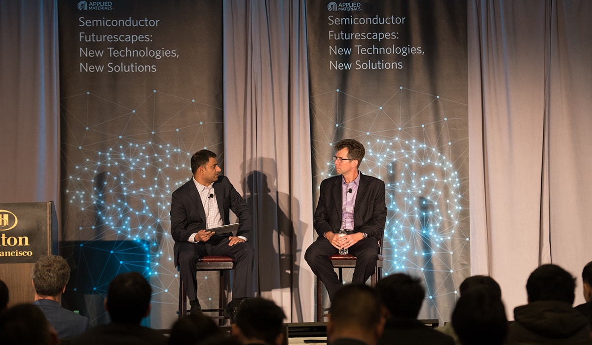
I had the pleasure of hosting an eye-opening presentation and Q&A with Dr. Jeff Welser of IBM at a recent Applied Materials technical event in San Francisco. Dr. Welser is Vice President and Director of IBM Research's - Almaden lab in San Jose. He made the case that the future of hardware is AI.
At Applied Materials we believe that advanced materials engineering holds the keys to unlocking commercial value from AI. We believe materials innovation will make possible a broader range of new processor and memory chips optimized for different types of AI workloads. This is necessary because traditional computing architectures consisting of CPU, SRAM for cache, DRAM and storage (HDD or SDD) may not be performance-, energy- or cost-optimal for new AI workloads. The rise of GPU and FPGA chips and custom architectures such as Google’s Tensor Processing Unit (TPU) are proof points for our AI thesis.
Here are three key takeaways from my Q&A with Dr. Welser:
- Beyond the current trend of using GPUs as accelerators, future advances in computing logic architecture for AI will be driven by a shift toward reduced-precision analog devices, which will be followed by mainstream applications of quantum computing. Neural network algorithms that GPUs are commonly used for are inherently designed to tolerate reduced precision. Reducing the size of the data path would allow more computing elements to be packed together inside a GPU, a dynamic that in the past was taken for granted as an outcome of Moore's Law technology scaling. Whether it is integration of analog computing elements or solving complex chemistry problems for quantum computing, materials engineering will play a critical enabling role.
- Addressing the processor-to-memory access and bandwidth bottleneck will give rise to new memory architectures for AI, and could ultimately lead to convergence between logic and memory manufacturing process technologies. IBM's TrueNorth inference chip is one such example of a new architecture in which each neuron has access to its own local memory and does not need to go off-chip to access memory. New memory devices such as ReRAM, FE-RAM and MRAM could catalyze innovation in the area of memory-centric computing. The traditional approach of separating process technologies for high-performance logic and high-performance memory may no longer be as relevant in a new AI world of reduced precision computing.
- AI computation in the form of training and inferencing will have to be pushed to edge devices and this will give rise to the burgeoning of systems of networks made up of computing devices. The majority of such edge devices would be power- and cost-constrained, so their computing requirements would likely only be met with highly optimized ASICs. It is too early to tell whether traditional fabless semiconductor companies would provide these types of ASICs, or if they will come from an entirely new class of companies, such as Cloud Service Providers. Figuring out optimal points for decision making within such networks, or ensuring that data are correctly tagged or bootstrapped to maximize learning ability, are two other highly complex problems that require further research.
Applied Materials is truly excited to be at the epicenter of making possible new computing models for AI. Stay tuned for future updates in this area and in the meantime, watch the video replay of the panel I moderated on Enabling the AI Era at Applied's 2017 Analyst Day.
Tags: AI, artificial intelligence, machine learning
Sundeep Bajikar
Corporate Vice President, Corporate Strategy and Marketing
Sundeep is Head of Corporate Strategy and Marketing (CSM) and guides the executive leadership team in the development of the company's growth thesis, strategic priorities, key initiatives and investor communications. He is also responsible for developing Applied’s marketing capabilities and community. Sundeep’s work served as the foundation for Applied’s strategies related to AI, ICAPS, Heterogenous Integration and Net Zero.
He joined Applied in 2017 after spending ten years as a Senior Equity Research Analyst covering global technology stocks, including Apple and Samsung Electronics, for Morgan Stanley and Jefferies. Previously he worked for a decade as a researcher, ASIC design engineer, system architect and strategic planning manager at Intel Corporation.
Sundeep holds an MBA in finance from The Wharton School and M.S. degrees in electrical engineering and mechanical engineering from the University of Minnesota. He holds 13 U.S. and international patents with more than 30 additional patents pending. Sundeep is also author of a book titled, “Equity Research for the Technology Investor – Value Investing in Technology Stocks.” He was an Institutional Investor Rising Star.
How to Think About Rising WFE Intensity
After declining significantly from a peak in 2000, wafer fab equipment (WFE) intensity has been on an uptrend in recent years. As a result, semiconductor equipment revenue growth has been outpacing semiconductor growth.

Battle of Exponentials — A Different Way to Think About Accelerating Semiconductor Growth
Semiconductor growth has accelerated to higher levels that may represent a new normal as suggested by our “battle of exponentials” framework.
Expanding the Ecosystem for Hybrid Bonding Technology
Applied Materials recently entered a new phase of our R&D collaboration with A*STAR’s Institute of Microelectronics to accelerate materials, equipment and process technology solutions for hybrid bonding and other emerging, 3D chip integration technologies.