Products & Technologies
Products & Services
Contact
Products & Services
Products & Technologies
Services
Resources
Contact
Posted
February 20, 2019

Stay updated on our content.
Innovations for Improving Patterning
Feb 20, 2019
The semiconductor industry’s leading experts in lithography, metrology, patterning technologies and materials will gather at the 2019 SPIE Advanced Lithography symposium being held from February 24 to 28 in San Jose. This annual forum is where discussions of the key patterning challenges and the latest advancements take place, providing a deeper understanding of new pathways to move the industry forward.
One of the biggest technical obstacles for device scaling is layer-to-layer vertical alignment or edge placement errors (EPE). EPE are patterning errors that result in the misalignment of critical features in multi-layer device designs. EPE can impact the yield of a chip, making layer-to-layer alignment an essential industry requirement. The urgent question is: what new technologies can be put in place to “see” through the layers and measure variation to control and reduce EPE at advanced nodes?
At this year’s symposium, Applied Materials will discuss techniques for minimizing EPE and other important developments. These include using new e-beam imaging technology for embedded defect detection, inspection and classification of EUV defects, and 3D pattern characterization.
Below is a guide to our papers and posters. We hope to see you at the conference!
SESSION 2: OVERLAY NEWS
Monday, February 25, 1:30 - 1:50 PM
On device EPE: minimizing overlay, pattern placement and pitch-walk in presence of EUV and etch stochastics, Applied Materials
SESSION PS1: POSTERS
Wednesday, February 27, 5:30 - 7:30 PM
Macro CD-SEM 2D metrology supporting advanced DRAM patterning process, Applied Materials
New imaging technique that enables detection of buried defects, Applied Materials
SESSION 12: DESIGN INTERACTIONS WITH METROLOGY
Thursday, February 28, 9:40 - 10:00 AM
3D optical proximity model optimization using in-line 3D-SEM metrology, Applied Materials, Synopsys GmbH (Germany)
SESSION 14: INSPECTION II
Thursday, February 28, 1:50 - 2:10 PM
SEM inspection and review method for addressing EUV stochastic defects, Applied Materials
Tags: Patterning, lithography, edge placement errors, EPE, metrology, e-beam
Applied Materials
Corporate Communications
The Applied Materials team publishes posts of general interest to our readers.
Now is the Time for Flat Optics
For many centuries, optical technologies have utilized the same principles and components to bend and manipulate light. Now, another strategy to control light—metasurface optics or flat optics—is moving out of academic labs and heading toward commercial viability.

Seeing a Bright Future for Flat Optics
We are at the beginning of a new technological era for the field of optics. To accelerate the commercialization of Flat Optics, a larger collaborative effort is needed to scale the technology and deliver its full benefits to a wide range of applications.
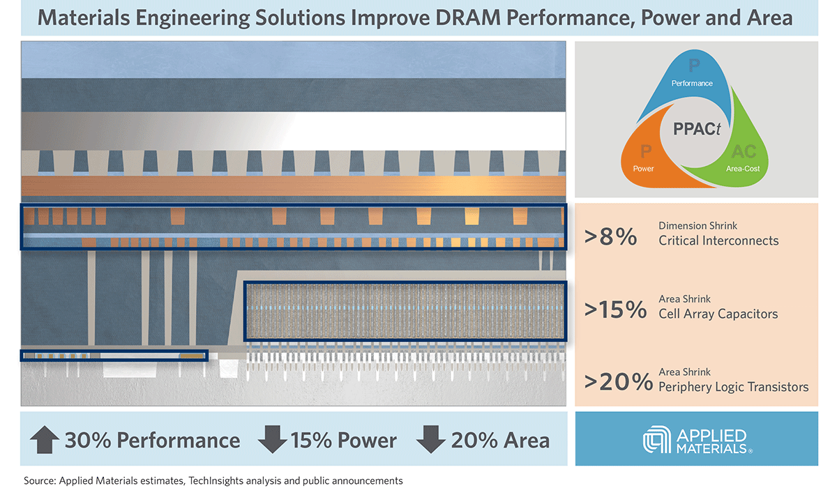
Introducing Breakthroughs in Materials Engineering for DRAM Scaling
To help the industry meet global demand for more affordable, high-performance memory, Applied Materials today introduced solutions that support three levers of DRAM scaling.