Products & Technologies
Products & Services
Contact
Products & Services
Products & Technologies
Services
Resources
Contact
Posted
June 29, 2023

Stay updated on our content.
Doubling Down on Collaboration at SEMICON West 2023

by Kevin Moraes
June 29, 2023
The semiconductor industry has proven itself more than capable of achieving growth by collaborating to overcome big challenges. Collectively, we have demonstrated innovation and resiliency that is fueling what several industry analyst firms project will be a $1 trillion semiconductor market by 2030 that could directly seed $3-4 trillion of global electronics growth[1].
To fulfill this opportunity in a responsible manner, we need clarity about the technical hurdles and our shared responsibility to build an increasingly sustainable semiconductor and electronics ecosystem. During the upcoming SEMICON West conference, held July 11-13 in San Francisco, Applied Materials will highlight our commitment to collaborating across the ecosystem to help lead the industry in developing solutions to increasingly complex challenges to future growth.
On Tuesday, July 11, Applied will host a Technology Breakfast event where we will introduce exciting new products and bring together industry leaders to discuss key technology inflections. As part of the program, we plan to launch our most significant semiconductor manufacturing platform innovation in more than a decade. Designed from the ground up to address the semiconductor industry’s most pressing challenges, this new modular platform will give chipmakers the utmost in flexibility, intelligence and sustainability – helping our customers manage manufacturing complexity, reduce carbon emissions and make progress toward net-zero initiatives.
The event will also feature a dynamic panel discussion on emerging trends in heterogeneous design and integration using advanced packaging technology. The panel will feature senior technology leaders from AMD, Intel and Qualcomm as well as leading hybrid bonding solution providers Besi and EV Group. The panelists will explain why and how heterogeneous integration will drive improvements in semiconductor and system performance, power efficiency, form factor and time-to-market.
Register now for this exciting event as it will fill up fast.
On Wednesday, July 12, Applied President and CEO Gary Dickerson will deliver a keynote as part of the SEMICON West session titled, “Path to Net Zero.” Gary will share Applied’s own carbon emissions data and playbook to reduce Scope 1, 2 and 3 emissions across the ecosystem. The “Collaborative Pathway to Net Zero” is based on partnerships with our suppliers upstream and customers downstream since collaboration is the key to Net Zero.
Achieving growth along with a better, more sustainable future requires companies from across the ecosystem to collaborate more than ever before. SEMICON West 2023 presents a great opportunity to raise, discuss and ultimately solve our industry’s most pressing growth challenges.
[1] McKinsey & Company, April 1, 2022: The semiconductor decade: A trillion-dollar industry
Kevin Moraes
Corporate Vice President, Strategy and Marketing, Semiconductor Products Group

Dr. Kevin Moraes serves as Corporate Vice President of Strategy and Marketing at Applied Materials, leading global initiatives that drive growth across key semiconductor segments. In this role, he aligns market insights with business priorities, shapes competitive positioning, and enables customer success through technology inflections. Previously, he held leadership positions in product management and technology development within the company. He earned a Ph.D. in materials science and engineering from Rensselaer Polytechnic Institute, an MBA from the University of California, Berkeley, and a bachelor’s degree in chemical engineering from Annamalai University.
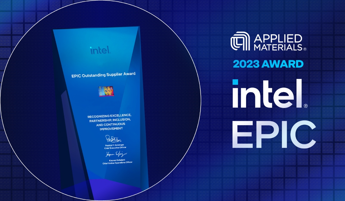
Applied Materials Earns Intel’s 2023 EPIC Outstanding Supplier Award with Supplier Diversity Distinction
Applied Materials has earned the exclusive Intel EPIC Program Outstanding Supplier Award with Supplier Diversity Distinction for 2023. This award recognizes the absolute top performers in the Intel supply chain for their dedication to continuous quality improvement, performance, collaboration and inclusion over the past year.
As Chipmakers Assess “Where” to Build New Fabs, the “How” of Semiconductor Innovation Must Remain a Priority
According to Ericsson, there are more than 6.5 billion smartphone users worldwide. I would speculate that very few of them have ever given much thought to what’s inside that phone — a miracle of science, engineering and manufacturing that is arguably one of humankind’s greatest technical accomplishments.
Bringing the Future of Advanced Patterning into Focus at SPIE
This year’s SPIE Advanced Lithography + Patterning conference comes at a time when the semiconductor industry needs new breakthroughs to solve the patterning challenges of continued scaling with EUV lithography which will become more intense with the arrival of High-NA EUV.