Products & Technologies
Products & Services
Contact
Products & Services
Products & Technologies
Services
Resources
Contact
Posted
October 04, 2019

Stay updated on our content.
Designing “Eyes” into Process Equipment to Improve Chip Performance and Yield

Oct 04, 2019
The AI Era of computing promises to improve society and create trillions of dollars in economic value. It arrives, however, at a challenging time for the semiconductor industry.
As Moore’s Law scaling has slowed, designers have explored new materials, integration schemes and structures that can deliver continued improvements in “PPAC”: chip performance, power and area/cost. Deploying these at good yield is challenging, particularly as process variability increases and tolerances shrink. To help accelerate customer roadmaps, Applied Materials is integrating metrology into process systems and chambers, bringing unprecedented granularity to wafer processing.
This type of integration is a logical next step for an industry that has been receptive to sensors, data and analytical process control. The number of sensors deployed in process systems has more than doubled over the past ten years, creating a wealth of data. Big Data and machine learning have improved, allowing more of the sensor data to be used in monitoring chamber health and even to predict on-wafer results in what we call “virtual metrology.”
To best control on-wafer and process results, there is still no substitute for taking direct measurements. For most processes, chipmakers have developed sampling strategies and used offline metrology and inspection to catch process deviations. CMP became an early candidate for integrated and in-situ sensors that enable real-time, on-wafer metrology and control.
Until recently, deposition systems have not needed in-vacuum, on-wafer measurement because of characteristics including:
- Process stability
- Wide process windows
- Thick unit films
- Simple process stacks
- Limited effects from exposure to the environment
Materials and integration schemes are changing rapidly, however, and this is why Applied’s engineers are putting “eyes” inside systems and chambers. In the AI Era, PPAC improvements are enabled by new and exotic materials and stacks. Interface engineering is at the atomic scale, and process success increasingly depends on “seeing” the wafer as it is being processed to ensure control and repeatability.
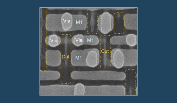
Applied recently introduced the Endura® Clover™ MRAM PVD platform, which is made up of nine unique wafer processing chambers that are integrated in pristine, high-vacuum conditions. This integrated materials solution includes on-board metrology (OBM) that measures and monitors the thickness of the MRAM layers—with sub-angstrom sensitivity—as they are being created. This ensures atomic-level control and prevents exposure to the outside environment. MRAM memories are made of sensitive materials that quickly degrade when exposed to impurities in the atmosphere. The critical control-layer of MRAM devices is extremely thin (as little as eight atoms in height), and film height uniformity of plus or minus a single atom is required to maximize device read performance and endurance.
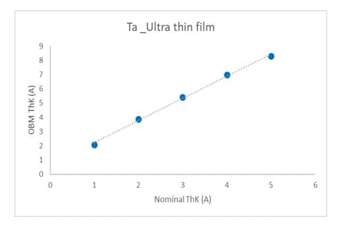
Figure 1: On-board metrology of ultra-thin Ta film produces exceptional linearity.
When processing ultra-thin films, any variability introduced by the measurement system can consume a significant proportion of the available process control budget. Long-term stability tests show that on-board metrology offers superior precision versus traditional, offline X-ray-based methods (figure 2).
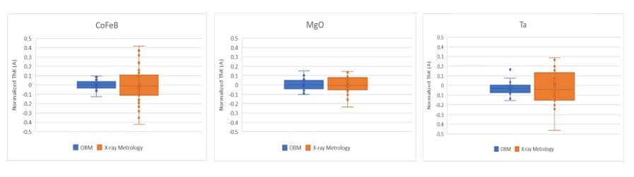
Figure 2: Long-term stability of critical MRAM films, on-board metrology versus offline x-ray metrology.
While on-board metrology is critical to achieving high yield in new memories such as MRAM, PCRAM and ReRAM, it can also bring advantages to 3D NAND and DRAM manufacturing. Inflections in logic are also driving the need to “watch” deposition processes to measure film thickness and uniformity as well as wafer geometry, stress, surface temperature and composition.
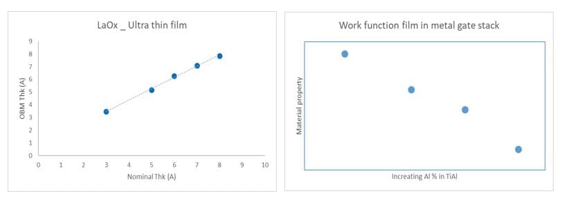
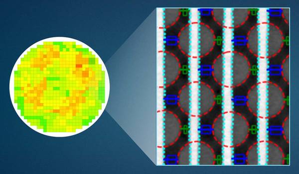
Figure 3: In-vacuum measurement of the thickness and material property of critical metal gate films.
It’s an exciting time for the industry. The AI Era is driving a renaissance in computing, and while classic Moore’s Law is slowing, new materials, integration schemes and structures are enabling advances in PPAC to continue. The unique requirements of the new and exotic materials are driving a renaissance in metrology. Applied’s goal is to give customers new capabilities that complement and extend offline metrology and virtual metrology models. By putting “eyes” in process systems and chambers, we can provide real-time monitoring and control on every wafer, helping customers maximize the performance of new chip designs and spot process deviations more quickly to improve yield.
Tags: AI Era, Moore's Law, MRAM, PPAC, metrology
Niranjan Khasgiwale
Vice President, Imaging and Process Control Group

Niranjan Khasgiwale is a vice president in the Imaging and Process Control group at Applied Materials, responsible for real-time measurement and control solutions. He has more than 20 years of marketing experience in the semiconductor equipment industry. Niranjan holds a master’s degree and Ph.D. in materials science from Dartmouth College and Lehigh University respectively, and a B.Tech in metallurgy from the Indian Institute of Technology.

Adding Sustainability to the Definition of Fab Performance
To enable a more sustainable semiconductor industry, new fabs must be designed to maximize output while reducing energy consumption and emissions. In this blog post, I examine Applied Materials’ efforts to drive fab sustainability through the process equipment we develop for chipmakers. It all starts with an evolution in the mindset of how these systems are designed.
Innovations in eBeam Metrology Enable a New Playbook for Patterning Control
The patterning challenges of today’s most advanced logic and memory chips can be solved with a new playbook that takes the industry from optical target-based approximation to actual, on-device measurements; limited statistical sampling to massive, across-wafer sampling; and single-layer patterning control to integrative multi-layer control. Applied’s new PROVision® 3E system is designed to enable this new playbook.
Breakthrough in Metrology Needed for Patterning Advanced Logic and Memory Chips
As the semiconductor industry increasingly moves from simple 2D chip designs to complex 3D designs based on multipatterning and EUV, patterning control has reached an inflection point. The optical overlay tools and techniques the semiconductor industry traditionally used to reduce errors are simply not precise enough for today’s leading-edge logic and memory chips.