Products & Technologies
Products & Services
Contact
Products & Services
Products & Technologies
Services
Resources
Contact
Posted
March 05, 2024

Stay updated on our content.
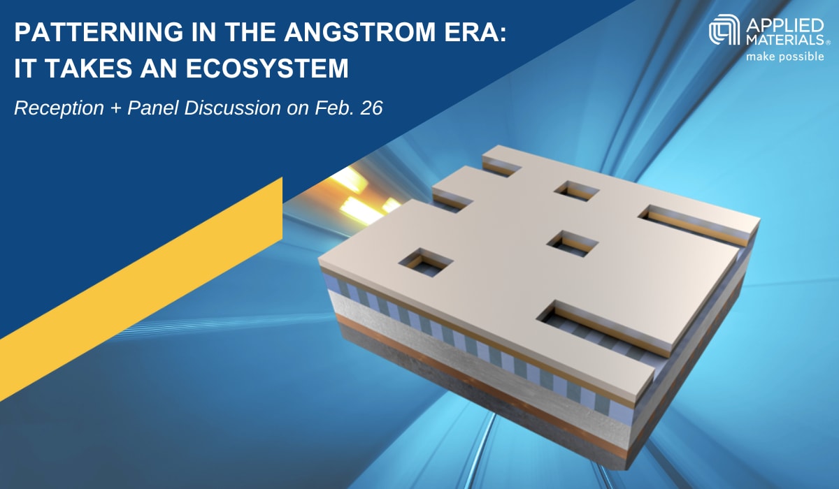
Collaboration is Key to Enabling Advanced Patterning in the Angstrom Era
by Regina Freed
March 5, 2024
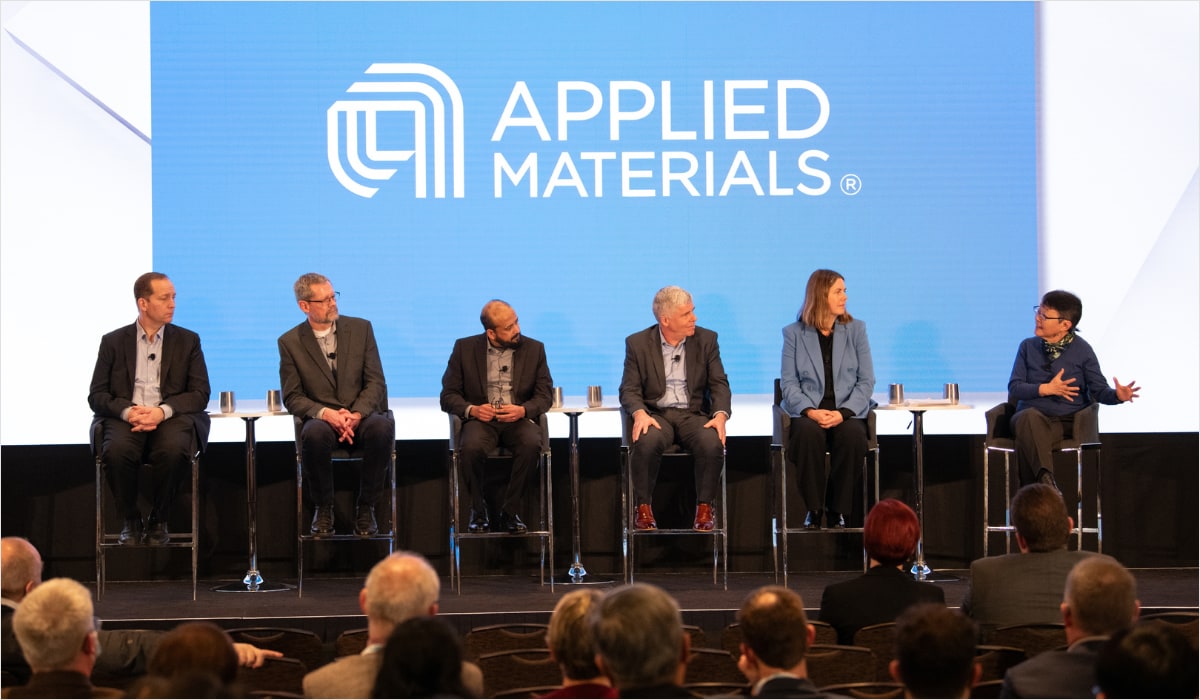
At the recent SPIE Advanced Lithography + Patterning Conference, Applied Materials hosted a panel titled, Patterning in the Angstrom Era: It Takes an Ecosystem, which delved deep into the changes coming to the patterning infrastructure across design, process and control. I was fortunate to be on the panel along with experts from NVIDIA, Intel, imec and Siemens EDA. One of the next big inflections in the semiconductor industry is the introduction of High NA EUV lithography and the panel was optimistic about the relatively smooth transition to this next-generation technology. At the same time, many important innovations in the adjacent patterning ecosystem are needed to support this transition.
A video replay of the panel is available on our SPIE 2024 event web page. Below is a brief summary of my key takeaways from the conversation.
Enabling the High NA EUV Transition
This year’s SPIE lithography conference comes on the cusp of a new era, where chipmakers are beginning to refer to chip features in terms of angstroms, not nanometers. High NA EUV will be used to print these ever-shrinking features, but there is one question on everyone’s mind: when will chipmakers adopt it?
Panel member Mark Phillips, an Intel Fellow and director of lithography hardware and solutions, said Intel expects to begin introducing High NA EUV in 2025. “The benefits of higher resolution are compelling in the right application,” Mark said, highlighting the potential for reduced process complexity, a shorter process flow, and more accurate edge placement. “Depending on the use case, moving to a numerical aperture of 0.55 will provide benefits in terms of better yield, cost and time-to-market.”
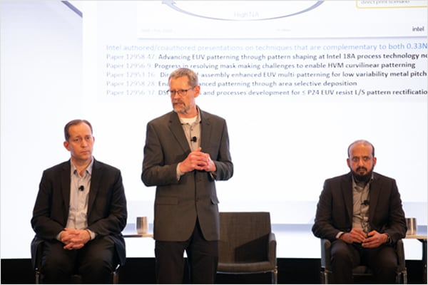
Mark Phillips, Intel
Mark said that in 2017, when the first-generation EUV systems were being developed, there were questions about the source power. His experience with this transition led him to say the same thing about High NA as he did back then: “It’s a matter of when, not if. If I take you back to 2017, those of us who were struggling with continuing to extend 193 immersion with more and more multi pattering, we knew we needed EUV and we had to go solve those problems with the source.”
Steven Scheer, senior vice president of advanced patterning, process and materials at imec, sees the transition to High NA EUV as an evolution, not a revolution. “The introduction of EUV obviously was a huge effort, a huge undertaking that took more than 10 years. The transition from 0.33 to 0.55 NA EUV is a more tractable problem,” he said. “It's a completely different timeline and the types of challenges that we see, they're all tractable problems that require work across the ecosystem in order to manage them. I think we'll work through those challenges and have a successful rollout of High NA EUV.”

Steven Scheer, imec
Supporting Seamless Stitching
Steven discussed a variety of changes needed to optimize High NA EUV patterning. High NA EUV uses anamorphic lenses, a difference in magnification in the X and Y directions, which results in half-field imaging. To image a full field, the two individual images must be stitched together. “There's a lot of interest from the industry to do that stitching at pitch, and that requires optimization simultaneously of the mask,” he said.
Steffen Schulze, vice president of product management for the Design to Silicon Division at Siemens EDA, said that chip architects are looking to the ecosystem to deliver field stitching without any design impact or special design rules for that area. “That's a very challenging task,” he said. “We know it will require more aggressive resolution enhancement techniques. It may require special mask rules in these areas.”

Steffen Schulze, Siemens EDA
Steffen said that, besides the ongoing effort to “confirm and harden” the stitching methodology, “there are discussions in the industry on having a large-field mask,” which would restore the ability to scan longer and to have the same chip sizes. He also took note of several talks at SPIE which focused on the impact of 3D integration, where smaller chiplets would be closely connected. “It seems there will be two streams, one that is revisiting the size of large chips versus an assembly of chiplets,” he said.
Kumara Sastry, distinguished engineer in the Advanced Technology Group at NVIDIA, said work is already underway to enable design of such large chips without stitching. “This work needs to be done, but I think it's not a showstopper,” Kumara said. “We do need as much flexibility as possible in terms of design rules and the size of the chips.”

Kumara Sastry, NVIDIA
Materials Innovation in the Angstrom Era
In this new era, we're clearly seeing the strong interdependence between lithography and materials engineering. The patterns on the EUV masks will not be the patterns on the wafers unless we tune all of the materials-related steps. As we start counting some dimensions in atoms, it becomes increasingly important to control the smoothness and strength of our chipmaking materials and how they interact with process chemistries or even with the light from the lithography stepper. There is a lot of work being done on material interfaces to make chips easier to produce at lower cost.
For example, at last year’s SPIE Lithography conference, Applied Materials introduced its Sculpta® pattern-shaping system, which reshapes EUV patterns to reduce spacing and increase density. This year, panel moderator Junko Yoshida, a longtime EE Times editor who now publishes The Ojo-Yoshida Report, asked if pattern shaping would play a significant role in the High NA EUV era. I explained that pattern shaping creates an extra degree of freedom, and can be used for several different purposes, such as bringing tip-to-tip spacing closer together, reducing the number of defects, or even eliminating stochastic bridge defects after they have formed – all of which makes processing more cost-effective so we can keep on scaling.
Junko Yoshida, The Ojo-Yoshida Report
Mark from Intel agreed, describing pattern shaping as “one of many techniques that are complementary to lithography.” He highlighted several papers at SPIE that feature complementary technologies designed to make lithography better. “In all cases, they allow you to do something more, they add value to your process, they make it more compelling, they push Moore’s Law a little bit further” he said.
At this year’s SPIE lithography conference, Applied shared new details about how chipmakers are deploying Sculpta systems in production, and we introduced a portfolio of supporting products in adjacent process steps. A press release and overview presentation are available on our SPIE 2024 event web page.
Big Data Means Big Opportunities
Besides the innovations in lithography and materials engineering, our industry has an opportunity to use advanced compute technologies to come up with new conclusions. Compute power and AI techniques will enable us to collaborate much more easily than in the past, to help narrow down a big problem to a smaller subset of problems so that we can innovate faster together.
“We have to use this accelerated computing and AI to help make our chips better, faster and at lower cost,” said Kumara from NVIDIA. “We need chips for accelerated computing and we need accelerated computing for chips.” He said increases in compute power speed up problem solving and “allow you to make fewer approximations so you can be much more rigorous and get to the answer, a more accurate answer, at the same time or even faster.” On top of this, machine learning and AI can deliver another order of magnitude in speed. “We can get faster info turns so that we can help accelerate fab development cycle time,” he said.
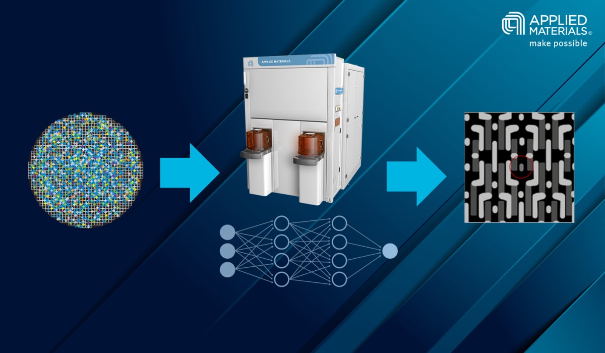
Kumara, whose focus at NVIDIA is on computational methods for advanced semiconductor manufacturing, shared an example from optical proximity correction, which is one of the largest workloads in the semiconductor industry. “Both in design and in manufacturing, [OPC] can be accelerated over 50x on a Hopper DGX system, and this in turn can accelerate a lot of info turns,” he said. Likewise in metrology, there was a time not long ago when 50-100 images were enough. “That's no longer the case,” he said, as AI/ML techniques can digest millions if not billions of images for defect identification.
Steffen from Siemens EDA highlighted another use case for accelerated computing and AI: increasing the accuracy of modeling and simulation. “As we go to smaller feature sizes, we are facing tighter accuracy requirements,” he said. “What we see today and I think will further grow is the transition to contour-based modeling, and the reason is that contours have much richer information to capture the complexity of the patterning process.”
It Takes a Village
The ultimate takeaway from this robust discussion is that we must work together across the entire ecosystem to continue driving progress in patterning. With these new levels of complexity and interdependency across design, process and control, no single company or even segment of the industry can do it alone. Thankfully, the semiconductor industry has a proud history of working together to overcome obstacles. As Kumara said, “If anything, this community – more than any community – has been shown to prove naysayers wrong.”
Regina Freed
Vice President, AIx™ Solutions

Regina Freed has more than 20 years of experience in the semiconductor industry, managing semiconductor process and equipment development for both logic and memory processes, including co-optimization between deposition and etch, lithography, metrology, and defect inspection. At Applied Materials, Regina leads our AIx™ program that enables us and our customers to accelerate development and ramp through Actionable Insights as well as control our processes to deliver improved process windows, enabling customers to scale faster and at lower cost, while optimizing device performance.
Advanced Patterning in the Angstrom Era: Challenges and Opportunities
As leading chipmakers begin ramping process technologies at two nanometers and below, the industry is entering a new era where chip features will be described by a different unit of measurement – the angstrom, or one-tenth of a nanometer.
Separating the Signal from the Noise: Combining Advanced Imaging with AI for Chip Defect Review
As leading chipmakers begin ramping process technologies at two nanometers and below, the industry is entering a new era where chip features will be described by a different unit of measurement – the angstrom, or one-tenth of a nanometer.
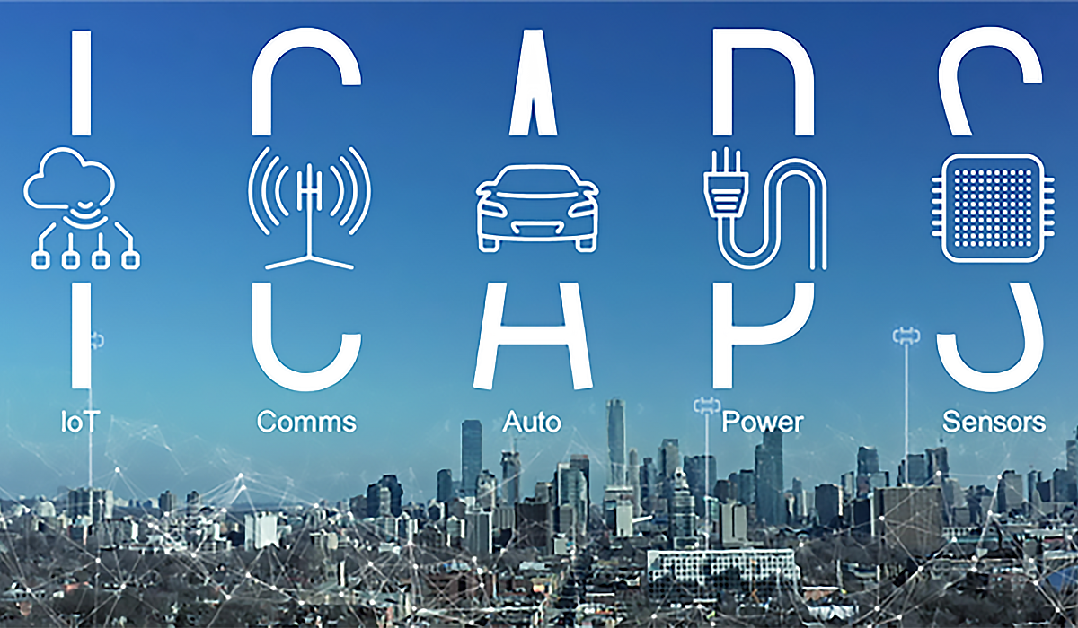
What’s Driving the Need for Innovation in ICAPS?
Applied Materials reached a significant milestone in 2023: For the first time, the largest portion of our wafer fab equipment sales came from customers in markets related to ICAPS – IoT, Communications, Automotive, Power and Sensors.