Products & Technologies
Products & Services
Contact
Products & Services
Products & Technologies
Services
Resources
Contact
Posted
July 09, 2018

Stay updated on our content.
Celebrating the Producer Platform’s 20 Years of Innovation
Jul 09, 2018
This month marks the 20th anniversary and 5000th shipment for one of the semiconductor industry’s most iconic and important manufacturing systems: the Producer® platform.
Launched in July 1998 as a single process system focused on chemical vapor deposition (CVD) to help enable the industry’s transition from aluminum to copper wiring, the Producer platform was designed from the ground up to provide customers the highest productivity and performance at the lowest possible operating cost.
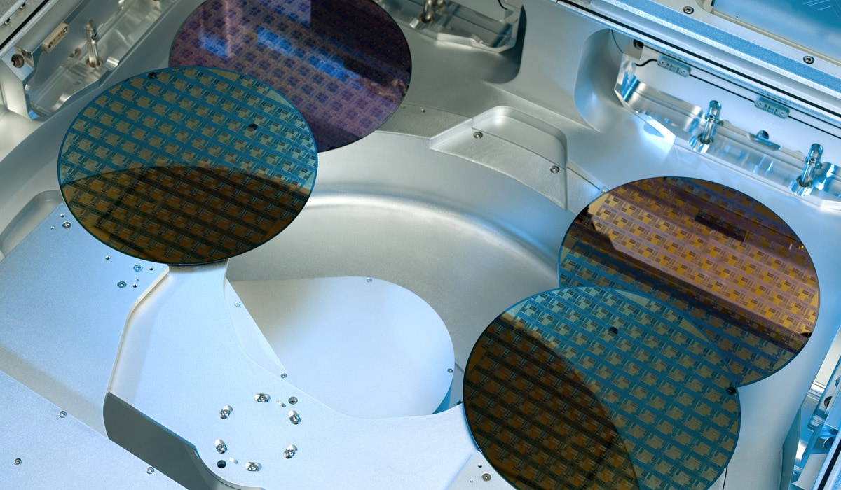
The Producer platform was revolutionary in concept, introducing the industry’s first twin process chamber architecture with single-wafer processing capability. With its unique capacity to process six wafers in parallel, the platform increased throughput by as much as 2x over the nearest competitor's system, particularly for thick CVD films. As a result, the Producer platform became an industry workhorse that has since taken on more tasks to help drive Moore’s Law and enable mass adoption of electronic products including notebook PCs, smartphones and wearable electronics.
Over the years, the Producer platform’s modular design and highly flexible architecture allowed it to continue evolving with expanded capabilities including etch, selective removal and treatment technologies. The platform helped enable several critical industry inflections including copper, strain engineering, high-k metal gate, FinFETs and most recently 3D NAND.
Today, on the dawn of the AI era, the Producer platform remains as important as ever amidst an incredible time of transformation for the semiconductor industry. AI workloads require new computing architectures and at the foundation is materials engineering. As more materials reach the physical limits of classic Moore’s Law scaling, Applied is pioneering development of new materials beyond the periodic table that enable continued improvements in chip performance and power efficiency. The Producer platform is key to this effort as it can now be used as an integrated process platform, offering various combinations of deposition and treatment, deposition and etch, or deposition and selective removal, in the same system and under vacuum.
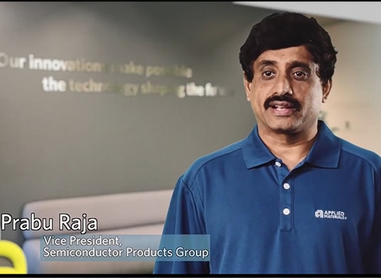
In the video below, Prabu Raja, senior vice president of the Semiconductor Products Group, celebrates this outstanding platform that helps make virtually every chip in the world. He highlights its industry stature and how it continues to deliver new solutions to enable the technologies shaping the future.
The Producer platform’s place in the history of the semiconductor equipment industry is undisputed and its success will endure.
Tags: Moore's Law, artificial intelligence, AI, materials engineering, video
Applied Materials
Corporate Communications
The Applied Materials team publishes posts of general interest to our readers.

Adding Sustainability to the Definition of Fab Performance
To enable a more sustainable semiconductor industry, new fabs must be designed to maximize output while reducing energy consumption and emissions. In this blog post, I examine Applied Materials’ efforts to drive fab sustainability through the process equipment we develop for chipmakers. It all starts with an evolution in the mindset of how these systems are designed.
Innovations in eBeam Metrology Enable a New Playbook for Patterning Control
The patterning challenges of today’s most advanced logic and memory chips can be solved with a new playbook that takes the industry from optical target-based approximation to actual, on-device measurements; limited statistical sampling to massive, across-wafer sampling; and single-layer patterning control to integrative multi-layer control. Applied’s new PROVision® 3E system is designed to enable this new playbook.
Breakthrough in Metrology Needed for Patterning Advanced Logic and Memory Chips
As the semiconductor industry increasingly moves from simple 2D chip designs to complex 3D designs based on multipatterning and EUV, patterning control has reached an inflection point. The optical overlay tools and techniques the semiconductor industry traditionally used to reduce errors are simply not precise enough for today’s leading-edge logic and memory chips.