Products & Technologies
Products & Services
Contact
Products & Services
Products & Technologies
Services
Resources
Contact
Posted
April 11, 2024

Stay updated on our content.
Building on an Unmatched Foundation of CVD Innovation
By Ajay Bhatnagar
April 11, 2024
In 1987, Applied Materials shipped the first Precision 5000 CVD (chemical vapor deposition) system – a breakthrough machine that revolutionized the deposition of the thin films at the heart of the chipmaking process. The internet was still a government research project and AI was the stuff of science fiction, but Applied’s innovative system laid the groundwork for many of today’s most advanced electronics applications. One of the most successful semiconductor manufacturing tools in history, the P5000 was inducted into the U.S. Smithsonian Institution’s exhibit on the Information Age for its importance to the evolution of the industry.
Flash forward more than three decades, and we recently celebrated the shipment of our 10,000th CVD system. Building on the legacy of the Precision 5000, Applied has introduced a steady stream of innovations in materials deposition that have helped enable several major industry inflections, such as low-k dielectrics, copper interconnects, strain engineering, high-k metal gate, FinFET transistors, and 3D NAND. At the recent SPIE Advanced Lithography + Patterning conference, Applied introduced the latest in its long line of CVD innovations, the Producer® XP Pioneer® CVD patterning film. This new deposition technology is aimed at accelerating the next generation of inflections in both memory and logic.
Driving DRAM Scaling
CVD has long played a role in enabling DRAM memory scaling. Early innovations targeted the gap fill process, which uses non-conducting materials to isolate individual DRAM transistors. Sub-atmospheric borophosphosilicate glass (BPSG) CVD films introduced in 1995 are still in production today at the most advanced nodes to create the mold material for DRAM capacitors.
In DRAM, data is stored as charges in cylindrical, vertically arranged capacitors that need as much surface area as possible to hold adequate numbers of electrons. As DRAM makers narrow the capacitors, they also elongate them to maximize surface area. Multiple support structures are needed to maintain the rigidity of the capacitors as they grow taller. Applied introduced a variety of new CVD films over the years to replace high-temperature furnace films, leading to significant share gains for the company in dielectric deposition products.
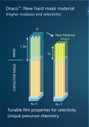
Taller capacitors also lead to another challenge: etching of deep capacitor holes threatens to exceed the limits of the “hard mask” material that acts as a stencil to determine where each cylinder is placed. If the hard mask is etched through, the pattern is ruined. To further enable capacitor scaling, Applied launched a novel hard mask called Draco™ in 2021. Draco is a new material that increases etch selectivity by more than 30 percent, thereby enabling a shorter mask stack and providing a dramatic improvement in local critical dimension uniformity of the capacitor holes. Draco has been co-optimized to work with Applied’s Sym3® Y HT etch system, which synchronizes etching with byproduct removal to enable patterning holes that are perfectly cylindrical, straight and uniform. The success of this co-optimization is a key reason why Applied’s share in DRAM has increased by 10 points over the past 10 years.
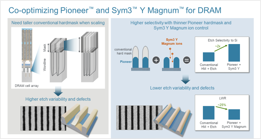
Demand for DRAM innovation continues to grow to feed the insatiable need for memory bandwidth in the AI era. The recently launched Pioneer CVD patterning film has already been adopted by leading memory manufacturers for DRAM patterning. Pioneer is a completely new CVD architecture based on a unique high-density carbon formula that is more resilient to etch chemistries used in the most advanced process nodes, permitting thinner film stacks with superior sidewall feature uniformity.
A thinner hard mask means less vertical distance is required for etch, resulting in a lower aspect ratio. This allows use of lower-power plasma and offers better control of the ratio of ions to radicals. A higher concentration of ions produces more efficient etches with better control, allowing desired patterns to be transferred to the wafer with exceptional fidelity. Pioneer is also being co-optimized with Applied’s new Sym3® Y Magnum® etch system to provide better control over conventional carbon films for critical etch applications in memory processing.
Enabling EUV Patterning
CVD is also critical in the lithographic patterning process. Around 2004, the first of Applied’s Advanced Patterning Films (APF) were introduced into the market. These thin amorphous CVD carbon films became an industry benchmark as hard masks for etching a variety of films with high selectivity. These transparent films required no alignment marks, which allowed for deep structure patterning. We continue to see a significant increase in APF layers today as advanced logic customers move from spin-on hard masks to denser CVD masks to improve pattern fidelity.
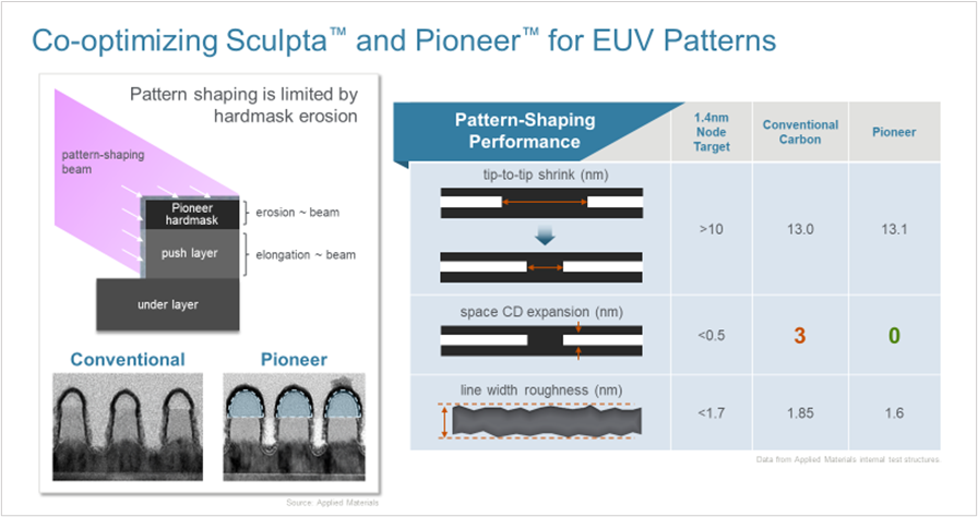
The move away from spin-on hard masks is accelerating as leading chipmakers transition to EUV lithography. Spin-on films do not have the density or modulus required for the ultra-fine dimensions printed by EUV systems. With our new Pioneer film, we have changed the molecular structure to increase the film’s density and stiffness, while also enhancing the selectivity of etching. The improved selectivity allows much smoother deposition of carbon films, which can provide a dramatic improvement in line edge roughness.
Pioneer has also been co-optimized with Applied’s Sculpta® pattern-shaping system. Pattern shaping uses an angled reactive ribbon beam, which can result in erosion of the top surface of the protective hard mask – impacting the ability to control dimensions of certain features and limiting the amount of shaping that can take place. When used in combination with Sculpta, the Pioneer CVD hard mask film enables further extension of patterns, with better control of critical dimensions.
The new Pioneer system strengthens Applied’s portfolio of CVD technologies, building on decades of leadership in a capability that is critical to the chipmaking process. Customers are already seeing the value of this innovative new system. Pioneer has achieved development and production tool of record positions at leading foundry-logic and memory customers, and we are on track to generate hundreds of millions of dollars in annual revenue in the coming years.
Ajay Bhatnagar
Managing Director, Global Product Management, Dielectric Deposition Products

Ajay Bhatnagar, Managing Director, has been leading global product management for Dielectric Deposition Products at Applied Materials since 2021 with responsibility for overall product management of dielectric patterning, blanket and gapfill films. He joined Applied in 1998 in the Dielectric Gapfill group working as a process engineer on the first 300mm SACVD BPSG systems. During his years at Applied, Ajay has held global product management positions in etch, selective removal products, dielectric gapfill and metal deposition products. He received his Ph.D. and M.S. degrees in material science and engineering from Stanford University.
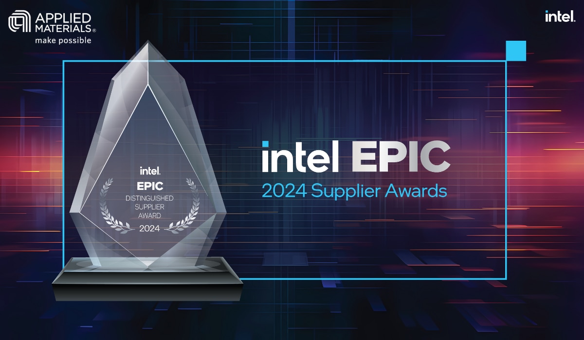
Applied Materials Earns Intel’s 2024 EPIC Distinguished Supplier Award
Applied Materials has earned Intel’s EPIC Distinguished Supplier Award. Through its dedication to Excellence, Partnership, Inclusion and Continuous (EPIC) quality improvement, Applied has achieved a level of performance that consistently exceeds Intel’s expectations.
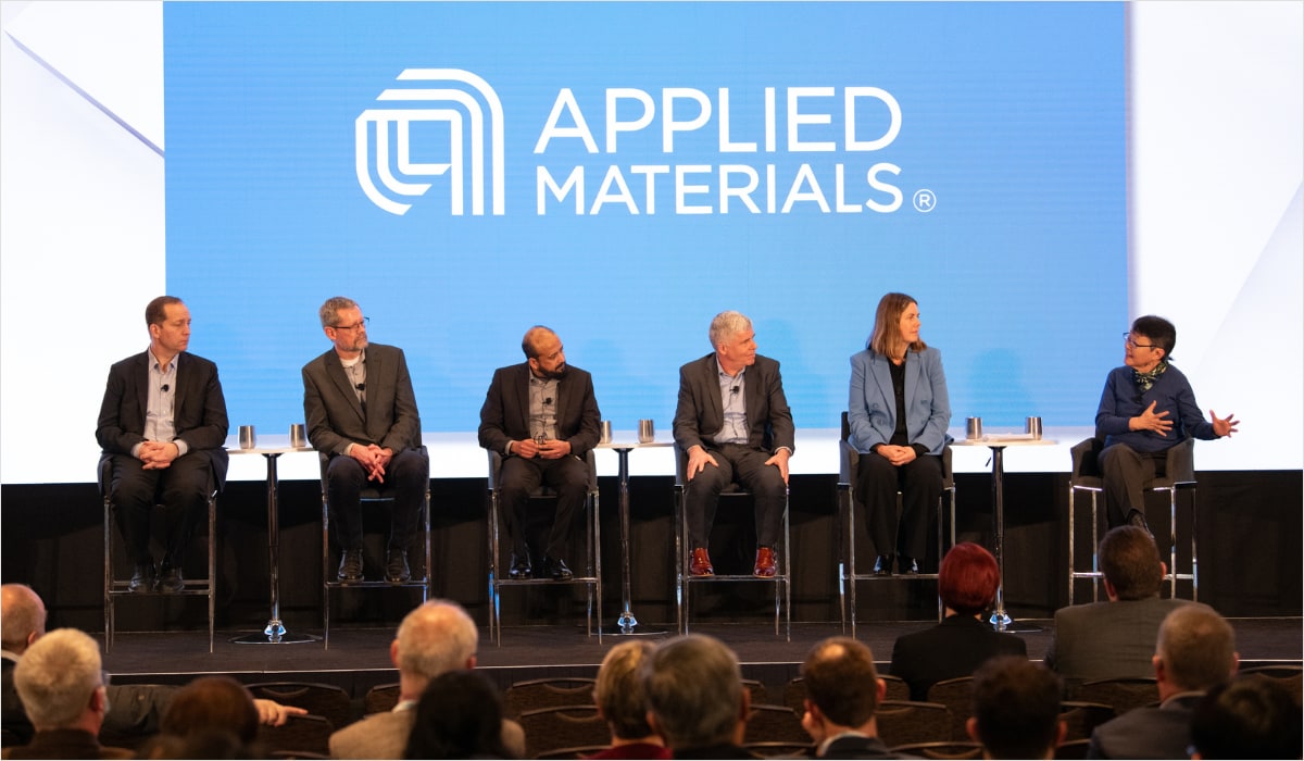
Collaboration is Key to Enabling Advanced Patterning in the Angstrom Era
At the recent SPIE Advanced Lithography + Patterning Conference, Applied Materials hosted a panel titled, Patterning in the Angstrom Era: It Takes an Ecosystem, which delved deep into the changes coming to the patterning infrastructure across design, process and control.
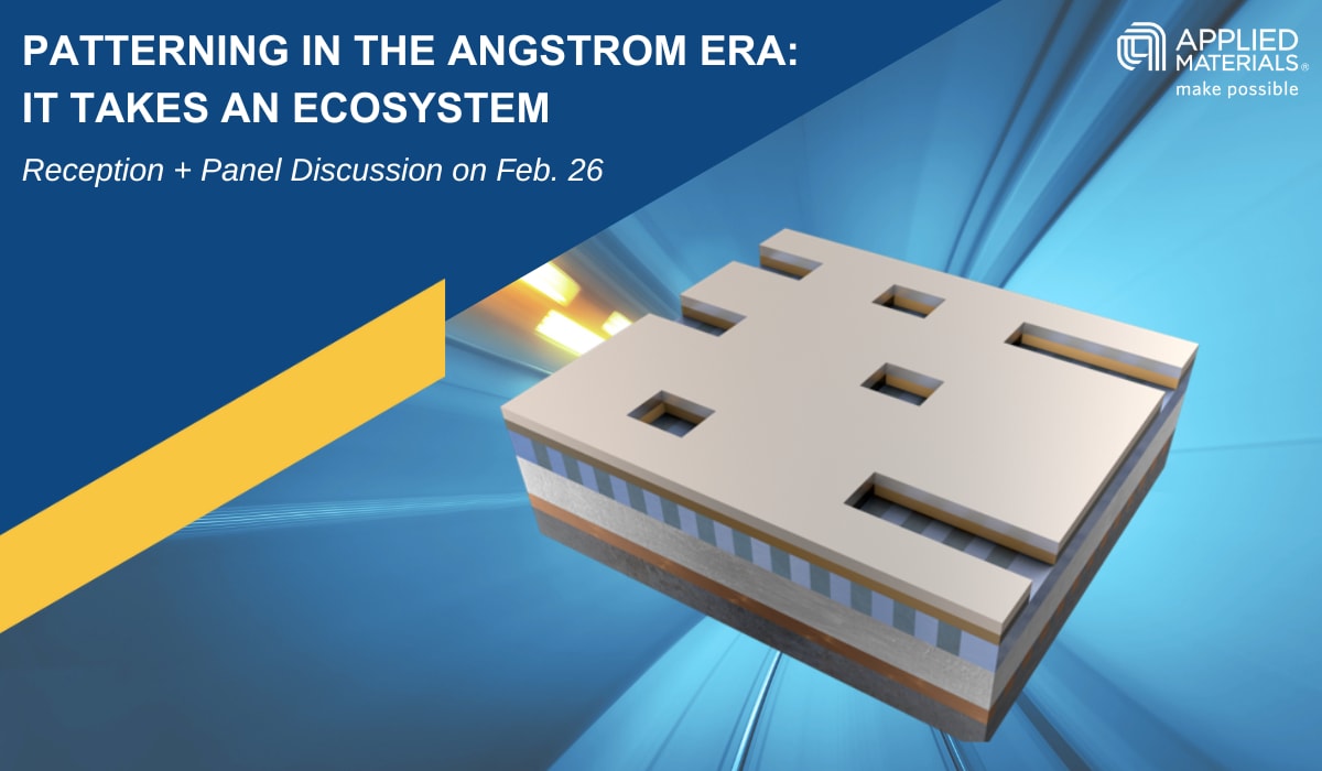
Advanced Patterning in the Angstrom Era: Challenges and Opportunities
As leading chipmakers begin ramping process technologies at two nanometers and below, the industry is entering a new era where chip features will be described by a different unit of measurement – the angstrom, or one-tenth of a nanometer.