Products & Technologies
Products & Services
Contact
Products & Services
Products & Technologies
Services
Resources
Contact
Posted
December 14, 2022

Stay updated on our content.
Bringing Next-Generation eBeam Technology Out of the Lab and into the Fab
by Ziv Parizat
Dec 14, 2022
Semiconductor complexity continues to increase with each new process node as the industry pushes the limits of 2D logic and DRAM scaling using EUV lithography and transitions to intricate 3D architectures including Gate-All-Around (GAA) transistors, high-aspect ratio DRAM and 3D NAND memories. This complexity creates significant challenges for process engineers. Defects become much more critical and difficult to detect as chip patterns shrink, the use of 3D structures proliferate and the number of layers increases. The ability to detect and characterize tiny, buried defects in emerging logic and memory chip designs is surpassing the imaging capabilities of conventional eBeam technology. In short, you can’t fix what you can’t see.
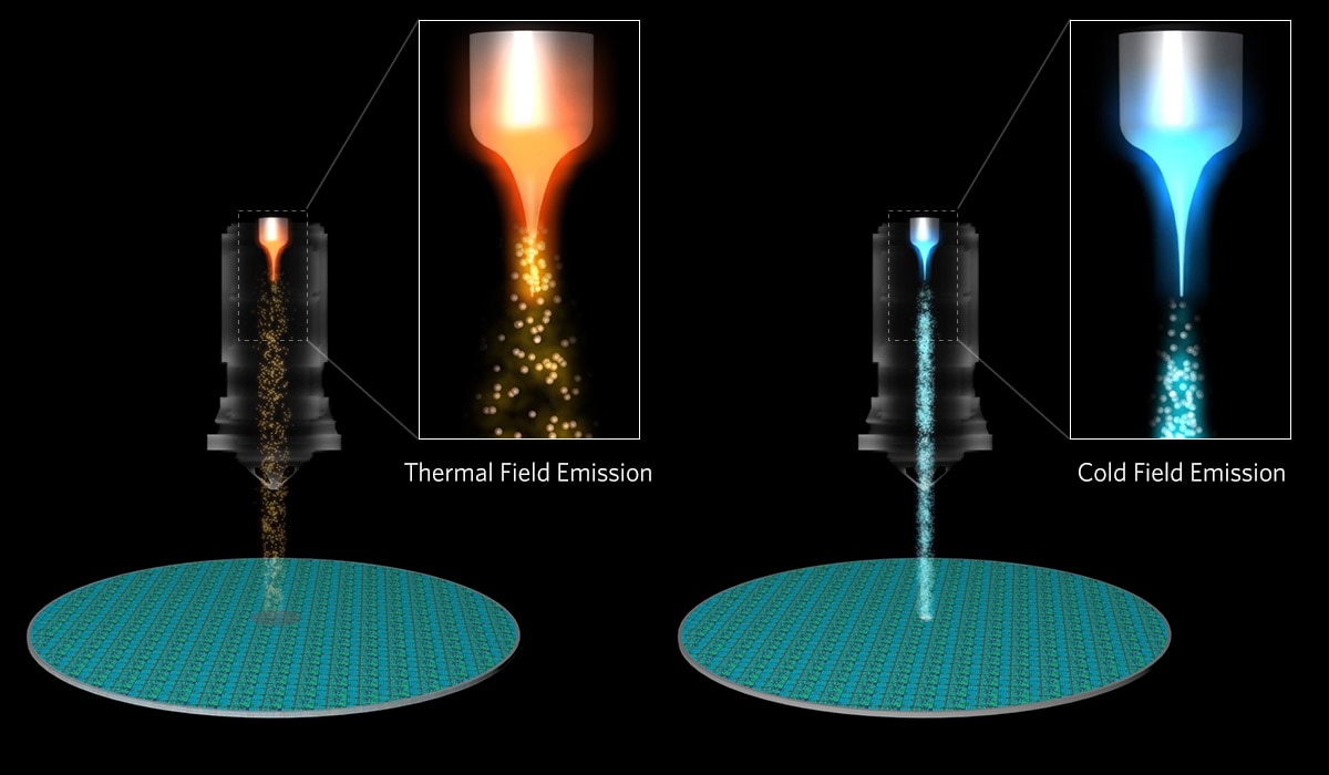
This is where cold field emission (CFE) technology comes in. Long regarded as the optimal eBeam technology, CFE operates at room temperature, resulting in narrower, higher-energy electron beams that produce higher resolution and faster imaging speed compared to conventional thermal field emission (TFE) technology which operates at temperatures exceeding 1,500 degrees Celsius. Process engineers can tune the CFE eBeam system for maximum resolution or they can lower the resolution to match that of TFE but with significantly faster imaging speed. The animation below illustrates the resolution and speed differences between CFE and TFE.
Until now, use of CFE-based systems has been limited to lab environments because the stability of the eBeam column was insufficient for the stringent requirements of high-volume semiconductor manufacturing. One of the main factors affecting stability is the cleanliness of the eBeam column. All eBeam systems contain an extremely small source tip that emits the electrons used for imaging. Because the tip is so small, any contamination – even a single atom – can potentially disrupt the flow of electrons and cause system instability.
In TFE systems, the source tip is so hot that it automatically repels any contaminants that might gather on the surface. In contrast, the room temperature operation of CFE, which is the main driver for its higher performance, makes cleaning much more challenging.
To bring CFE technology out of the lab and into the fab, Applied’s engineers and technologists developed two innovations that solved the CFE stability challenge. The first was creating an extreme ultra-high vacuum inside the eBeam column that is well below 1 x 10-11 millibar, which is two to three orders of magnitude better than for TFE systems and nearly the vacuum level found in outer space! Through an extensive optimization process, Applied combined an extreme ultra-high vacuum with specially developed chamber materials to greatly reduce the presence of contaminants inside the eBeam column.
Even under extreme ultra-high vacuum, a tiny amount of residual gas can still exist. If gas molecules adhere to the electron source, performance is significantly degraded. The second innovation we developed is a cyclical self-cleaning process that continuously removes contaminants from the CFE source, thereby enabling stable and repeatable performance for high-volume manufacturing environments.
As explained in the video below, commercializing Applied’s CFE eBeam technology took more than 10 years of intense development and collaboration between our teams located in Israel and Germany. The result is today’s introduction of our first CFE-based eBeam products – the SEMVision® G10 for defect review and PrimeVision® 10 for defect inspection.
By enabling customers to discover defects they’ve never been able to see before, faster, Applied is helping accelerate the development and production of advanced process nodes.

Ziv Parizat
Head of Marketing, Process Diagnostics and Control (PDC)

Ziv Parizat leads marketing for the Process Diagnostics and Control (PDC) group at Applied Materials. He joined Applied in 2005 and holds a B.Sc in bio-medical engineering from Tel Aviv University, and M.E. in systems engineering from the Israeli Institute of Technology (Technion).
Subscription Services Provide Increased Value to Chipmakers
For chipmakers, being early to market with industry-leading technology is extremely valuable. It can directly impact market share, revenue and gross margin. The faster chipmakers can reach high-volume manufacturing, the sooner and higher the return on their fab investment.
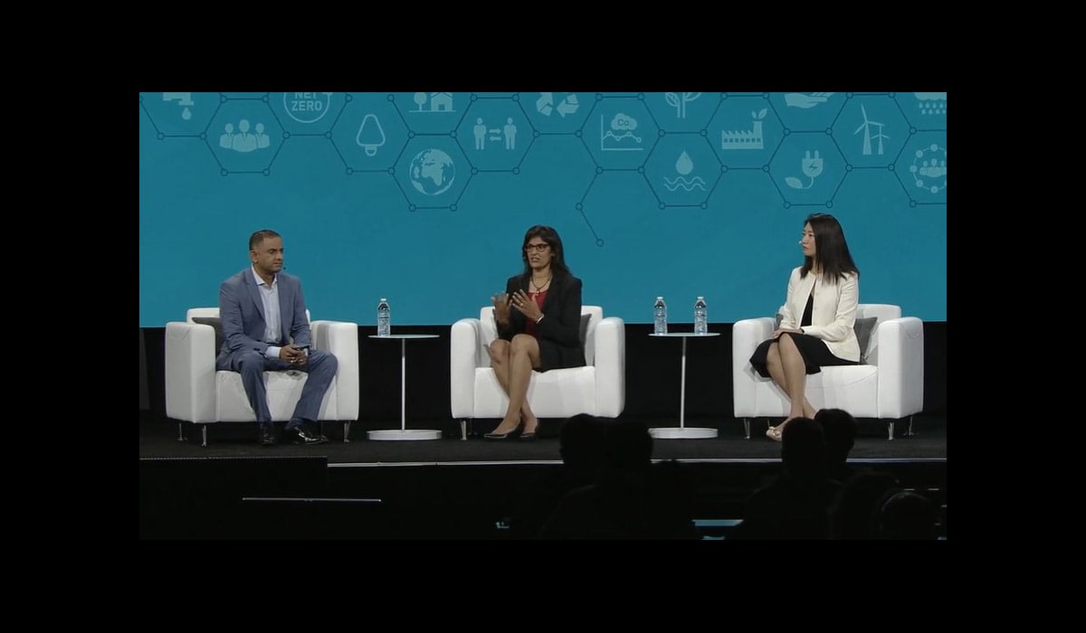
Takeaways from Panel Discussion at Sustainability Summit
I enjoyed hosting a panel discussion with my colleague Nasreen Chopra, who leads the Systems Engineering Center of Excellence for Applied’s Semiconductor Products Group, and Betty Jiang, head of U.S. ESG Research at Credit Suisse, as part of the Semicon West Sustainability Summit.

Greater Collaboration and Transparency in Reporting are Key to a More Sustainable Semiconductor Industry
The threat posed by climate change is motivating efforts around the world to improve corporate sustainability, reduce greenhouse gas (GHG) emissions and limit global temperature rise to 1.5°C under the Paris Agreement.