Products & Technologies
Products & Technologies
Services
Resources
Posted
February 27, 2019

Stay updated on our content.
Beyond Von Neumann: Moore's Law and the Shift from Near-Memory to In-Memory Compute

Feb 27, 2019
In reflecting a little bit on my last blog, it probably would have been good to do a little bit of explaining around what Von Neumann computing is, before discussing what’s beyond it. However, a bit of background on Moore’s Law is in order first.
We’ve made tremendous progress as an industry in decreasing the size, cost and power requirements of chips concurrently through Moore’s Law scaling. Between 1956 with the Univac I (1,900 floating-point operations per second for 125 kW) and the supercomputers of today (Wikipedia cites tests on a RIKEN at 6673.8 MFLOPS/watt), we’ve decreased the power cost of a floating-point operation by roughly a factor of 400 billion—that’s a difficult number to grasp. To put this in perspective, let’s consider another performance-per-power analogy, specifically mileage-per-gallon: if we started from a baseline of 15 mpg with the Model T and improved this by a factor of 400 billion, cars could go 6 trillion miles on a gallon, which is roughly one light year or a quarter of the distance to the nearest star, or have enough gas to make round trips to Pluto more than 500 times. Cars would also cost less than a penny.
This triple win of power-cost-performance from scaling (or making things smaller costs less because it uses less silicon and less power for the same performance) has allowed the industry to be less reliant on disrupting the traditional Von Neumann compute paradigm. Von Neumann computing, at its heart, is about taking input data and moving it between memory where it’s stored and logic where it’s manipulated to the rhythm of a clock. All data is stored in memory and then transported to a calculation engine. Shuttling around all this data carries with it a significant power and performance tax that’s largely been masked due to the astounding progress made through Moore’s Law scaling. Additionally, if we think about the Von Neumann clock ticks or compute cycles, the physical movement of the data takes more energy and compute cycles than the actual computation. The separation of memory and logic is core to the Von Neumann paradigm, but biology figured out a better way—doing the compute in memory.
When you look at the latest product descriptions for GPUs or for CPUs, it becomes clear that the focus and marketing are on how much memory is incorporated locally or on chip. Chips work faster and perform better if they can cycle the data locally or on chip a few times before having to send data via the motherboard all the way back to DRAM or non-volatile storage. There are many clever ways to improve the power efficiency of the Von Neumann paradigm that all involve “near memory”—getting memory elements closer to logic elements. Packaging different chips together in very close proximity and putting more memory on die are vectors that Applied Materials is also actively engaged on supporting.
While the industry has made great progress improving the power efficiency of computing, biology has architected a far more power-efficient strategy; in the brain, we store data in the same place where we do the compute. I’m told we either check the weighting at a typical synapse/neuron and/or tweak its value and all of them work in parallel to drive biological logic. This is far more power efficient than constantly moving things back and forth between two discrete environments.
Ultimately, the goal of our project funded by DARPA as part of the Electronics Resurgence Initiative (ERI) is to take systems beyond the Von Neumann architecture to “in-memory compute.” By having a correlated electron element that can be programmed to a discrete resistance value and state, and then convolving these elements with different weightings to one another we can build systems that approximate synapses and neurons. If we take memory elements and organize them into an array we can program elements, leveraging the right engineered materials to different resistance values. In this arrangement we can organize many weight values (based on the resistance of the element) and interrelate them via the array. This gets us closer to the efficiency of a biological system.
In many respects, the challenge isn’t in developing the paradigm; it’s in developing materials that can enable the paradigm. There are multiple vectors Applied Materials is pursuing to enable neuromorphic compute through materials innovation, with our correlated electron work being one of the many materials-enabled approaches.
Since I’ve last updated you, the team has been doing great work diligently preparing upwards of 1,800 different samples of many different compositions, with a lot of help on evaluating the electrical characteristics and the directions to explore by our collaborators at the University of British Columbia, the University of Colorado Boulder, Arm and Symetrix. We’re getting close to narrowing down to a specific materials system for the second phase of our project and I look forward to updating you again on our progress in the next couple of months.
Tags: neuromorphic computing, Von Neumann, DARPA, Moore’s Law, memory
David Thompson
Chemist, Discovery and Identification

David Thompson leads a team of chemists at Applied Materials tasked with supporting the discovery and identification of chemistries for new differentiated tool offerings. He did his undergraduate studies in chemical engineering and received a Ph.D. in the organometallic chemistry of fullerenes and nanotubes. Both of these degrees were obtained at Queen’s University in Kingston, Ontario, Canada. David has 56 granted US patents in semiconductor chemistry, process, and integration.

Now is the Time for Flat Optics
For many centuries, optical technologies have utilized the same principles and components to bend and manipulate light. Now, another strategy to control light—metasurface optics or flat optics—is moving out of academic labs and heading toward commercial viability.

Seeing a Bright Future for Flat Optics
We are at the beginning of a new technological era for the field of optics. To accelerate the commercialization of Flat Optics, a larger collaborative effort is needed to scale the technology and deliver its full benefits to a wide range of applications.

Introducing Breakthroughs in Materials Engineering for DRAM Scaling
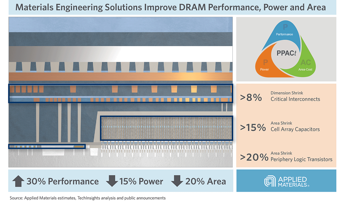
To help the industry meet global demand for more affordable, high-performance memory, Applied Materials today introduced solutions that support three levers of DRAM scaling.
