Products & Technologies
Products & Services
Contact
Products & Services
Products & Technologies
Services
Resources
Contact
Posted
May 16, 2023

Stay updated on our content.
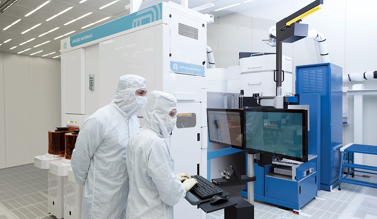
As Chipmakers Assess “Where” to Build New Fabs, the “How” of Semiconductor Innovation Must Remain a Priority
by Tristan Holtam
May 16, 2023
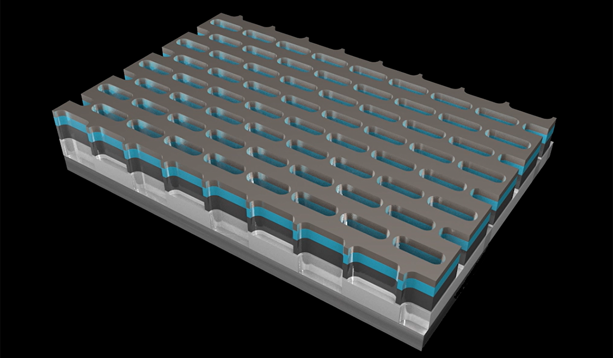
According to Ericsson, there are more than 6.5 billion smartphone users worldwide.1 I would speculate that very few of them have ever given much thought to what’s inside that phone — a miracle of science, engineering and manufacturing that is arguably one of humankind’s greatest technical accomplishments. As small as a child’s fingernail and no thicker than a sheet of paper, a state-of-the-art silicon chip contains 15 billion individually controlled switches connected together with 60 miles of wiring. It is built from 25 materials combined in a hundred different ways, the thinnest layer of which is just four atoms thick. What’s equally amazing is we can mass-produce those chips at a price point that has put incredibly powerful technologies into the hands of billions of people all around the globe.
The impact of semiconductors on the world has been profound and today there is an insatiable appetite for silicon. Over half a trillion dollars of chips were sold in 2022 and, as we enter a new age of computing powered by smart devices, big data and artificial intelligence, the industry is on a path to reach a trillion dollars by the end of the decade. Digital transformation of the economy will touch almost every aspect of our lives — from healthcare to research, retail, transportation, education, manufacturing, and agriculture. This digital transformation of the economy is built upon semiconductors, and that means chips are more strategically and economically important than ever.
Challenges: The Five Cs
Complexity: Technology complexity of chips is increasing significantly as traditional 2D scaling slows and the industry transitions to a new playbook to drive improved performance, power, area-cost and time-to-market.
Cost: The complexity of the industry roadmap is increasing costs with every node, and driving higher spending on R&D.
Cadence: The time needed to develop, commercialize and bring new technologies to high-volume manufacturing is expanding.
College Grads: The industry growth potential is threatened by shortfalls in the talent pipeline.
Carbon Emissions: The environmental impact of the industry’s value chain is set to quadruple in the next 10 years, if left unaddressed.
Around the world, governments are understanding the critical role semiconductors play in the economy and society. In the United States, this national imperative is most visible in the CHIPS and Science Act — a bipartisan initiative that is seen as both a matter of economic and national security as well as a recognition of the criticality of the semiconductor supply chain. Funding from the CHIPS Act will allow chip companies to make larger investments sooner, and by accelerating spending in new manufacturing capacity, we will create a more resilient supply chain to support many U.S. industries.
But semiconductor leadership is not just about where chips are made. It is also critical to lead in how chips are made — the foundational technologies that will define the next generation of semiconductors. In other words, we don’t just need more chips, we need better chips that are faster, smaller, use less power and are even more affordable. But the laws of physics and economics are getting in the way; it’s a classic case of what got us here, won’t get us to where we want to go.
The complexity of next-generation chip technology is simply mind-boggling. The physics, materials science and precision are extreme. Complexity drives up costs and extends the time it takes to bring new solutions to market. It also contributes to the industry’s carbon footprint. Left unmitigated, carbon emissions generated by the semiconductor value chain could quadruple this decade with half the incremental impact coming from increased complexity and the other half from growing production volumes.2 There are other challenges too, specifically shortfalls in the talent pipeline. A recent study by Deloitte forecast that, to support its growth, the global semiconductor industry will need to add more than one million additional skilled jobs by 2030.3
Addressing these challenges is paramount if we are to realize the immense promise of future chip technology. At Applied Materials, we believe this boils down to two crucial things — innovation and collaboration. For us, this is not just philosophy; we are making significant, strategic investments in new R&D infrastructure that can act as a catalyst to change the way chipmakers, universities and industry partners work together. Our goals are to increase the speed of innovation and commercialization, reduce the cost of bringing new manufacturing technologies to market, and inspire the next generation of innovators.
The next era of chipmaking will be shaped by incredible opportunity and tremendous complexity. It calls for bold, inclusive solutions. By bringing together the best and brightest from everywhere, breaking down traditional silos, and forging new models for collaboration based on deep and enduring trust, we can open up endless new possibilities. Stay tuned to learn more about Applied’s vision of the future — it’s going to be epic and it’s closer than you think.
1 Ericsson Mobility Report, November 2022
2 Imec/SEMI
3 The Global Semiconductor Talent Shortage, Deloitte, 2022
Tristan Holtam
GVP, CEO Chief of Staff, Corporate Strategy and Development

Tristan Holtam is group vice president and chief of staff to the President and CEO of Applied Materials, Inc., Gary Dickerson, where he plays an important role in developing and communicating Applied’s vision and strategy. As head of Corporate Strategy and Development, he works across the business groups and functions to manage the company’s strategy development process and operating rhythm. His responsibilities span key functional groups including corporate strategy and marketing, communications and public affairs, government relations, and facilities. In addition, he oversees teams that are incubating new strategic capabilities and growth opportunities for the company.
Mr. Holtam started at Applied as a New College Graduate in 1997, working in product development and management roles in the Semiconductor and Energy and Environmental Solutions groups before joining the corporate staff.
Mr. Holtam earned his bachelor’s degree in mechanical engineering from the University of Surrey, UK, an MBA from Henley Business School and has been awarded nine patents.

Semiconductor Industry Sustainability Priorities – A Systems Engineering Opportunity
Reducing emissions and optimizing resources in semiconductor manufacturing is an immensely complex undertaking, with multiple moving parts and several cascading impacts. While semiconductors are key to enabling a sustainable future, fabricating those chips is a notoriously resource-intensive process.
Bringing the Future of Advanced Patterning into Focus at SPIE
This year’s SPIE Advanced Lithography + Patterning conference comes at a time when the semiconductor industry needs new breakthroughs to solve the patterning challenges of continued scaling with EUV lithography which will become more intense with the arrival of High-NA EUV.

Bringing Next-Generation eBeam Technology Out of the Lab and into the Fab
Semiconductor complexity continues to increase with each new process node as the industry pushes the limits of 2D logic and DRAM scaling using EUV lithography and transitions to intricate 3D architectures including Gate-All-Around (GAA) transistors, high-aspect ratio DRAM and 3D NAND memories.