Products & Technologies
Products & Technologies
Services
Resources
Posted
May 10, 2024

Stay updated on our content.
Applied Materials Showcases Memory Innovations at IMW 2024

by Gill Lee
May 10, 2024
Large language models (LLMs) have been around for years, but they only recently entered the popular lexicon with the launch of ChatGPT and the ensuing generative AI boom. While many are now familiar with the concept of LLMs, they may not realize just how much memory is required to store and process these massive models. Innovation in memory technology has an important role to play in the continued growth of generative AI.
At Applied Materials, we have been investing in technologies to drive memory innovation for decades. That’s why we have a continually strong presence at the annual IEEE International Memory Workshop. This year is no different – Applied technologists will be showing up in force at IMW 2024, which will be held in Seoul, Korea from May 12-15. IMW is the premier forum where engineers and researchers from around the world explore the latest developments in memory technology.
IMW is not just focused on new memory devices and architectures, but also the high-volume process and packaging technologies that enable them. Applied is the leading provider of process equipment for compute memory, supplying a broad range of systems to all of the leading memory chipmakers. At IMW 2024, we will showcase advances in process equipment and technologies with four papers that highlight the importance of materials engineering to innovation across the entire memory hierarchy, from compute memory to storage and beyond.
Die-to-Wafer Hybrid Bonding Challenges for High-Bandwidth Memory
To support the computational intensity of generative AI workloads, chipmakers have recently turned to high-bandwidth memory (HBM) – an architecture that leverages 3D stacks of DRAM to enable the high-bandwidth, low-latency data access needed for AI parallel processing. Currently, HBM packages stack DRAM dies using thermocompression or flip-chip bonding with copper pillars. This invited paper, which will be jointly presented with Applied’s development partner BE Semiconductor Industries N.V. (Besi), explores the emerging transition to die-to-wafer (D2W) hybrid bonding, which eliminates the need for copper pillars by directly bonding the die surfaces onto a target wafer. In this presentation, Applied and Besi will discuss the key requirements for a successful D2W hybrid bonding process, including unique challenges for memory stacking including alignment, thin-die handling, and frontside and backside surface preparation. The team will highlight advancements made toward development of the industry’s first fully integrated equipment solution.
Demonstration of High-Growth-Rate Epitaxially Grown Silicon Channel on 3D NAND Vehicle with Memory Functionality
While HBM DRAM is primarily used as memory for high-performance compute applications, 3D NAND flash has been widely deployed as storage memory in a range of consumer devices such as tablets, laptops and smartphones. The density of 3D NAND memory chips has dramatically increased through the vertical stacking of wordline layers, aiming to accommodate more cells within a limited footprint. Despite these advancements, mainstream 3D NAND architectures are still built with polysilicon channels, which are prone to defects that can significantly increase channel resistance, especially as more cells are connected in series. A new approach to channel design becomes increasingly crucial for each subsequent technology node. In this paper, Applied engineers explore single-crystalline epitaxial silicon as an alternative channel material that holds promise for overcoming existing challenges and pushing the boundaries of 3D NAND technology.
Gate-All-Around SRAM: Performance Investigation and Optimization Towards VCCmin Scaling
Within the memory hierarchy, SRAM is the fastest and closest to the processor – typically integrated on the same system-on-chip (SoC). While the dimensions of logic devices have continued to scale aggressively, SRAM scaling has slowed and can impose a limitation on the minimum operating voltage and standby leakage for the entire SoC, thereby affecting energy efficiency. The industry transition from 3D FinFET transistors to Gate-All-Around (GAA) architectures presents an opportunity to renew SRAM scaling. In this paper, Applied engineers use advanced modeling techniques to compare the performance of FinFET SRAM to GAA SRAM. Results show that GAA SRAM can have better stability, writability and read-current compared to FinFET SRAM, while also achieving lower operating voltages, which can lead to an overall improvement in the energy efficiency of the SoC.
Self-rectifying Non-volatile Tunneling Synapse: Multiscale Modeling Augmented Development
Applied’s final paper at IMW explores an entirely new type of architecture called in-memory computing, which allows processor operations to be performed within computer memory. To enable the transition to in-memory computing, researchers are developing a new type of memory building block modeled after the synapses that connect the billions of neurons in a human brain. A key enabler of this transition will be the introduction of a large number of new materials combined in innovative ways to create the synaptic memory cells. In this paper, the Applied team presents a bottom-up device development methodology leveraging multiscale physics simulations to screen material and process combinations. The team also engineered a synaptic device and validated it in silicon, enabling the assessment of process integration tolerances.
Gill Lee
Managing Director, Technical Marketing / Strategic Programs - Semiconductor Products Group

Gill Lee is managing director of technical marketing / strategic programs in the Semiconductor Products Group at Applied Materials. He joined Applied in 2009, having worked previously in memory technology development at Qimonda/Infineon/Siemens in New York, France and Germany. Gill earned his M.S. in materials science and engineering from POSTECH University, South Korea. He has authored a number of papers on CMOS integration and process development and holds several related patents.

Building on an Unmatched Foundation of CVD Innovation
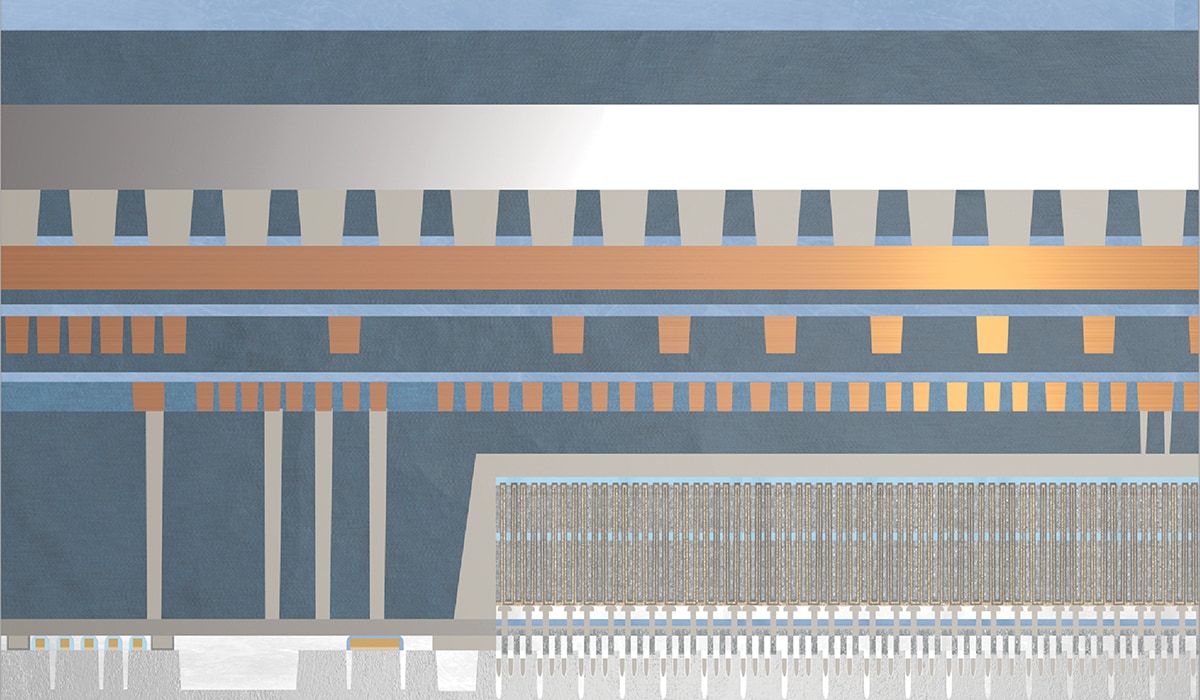
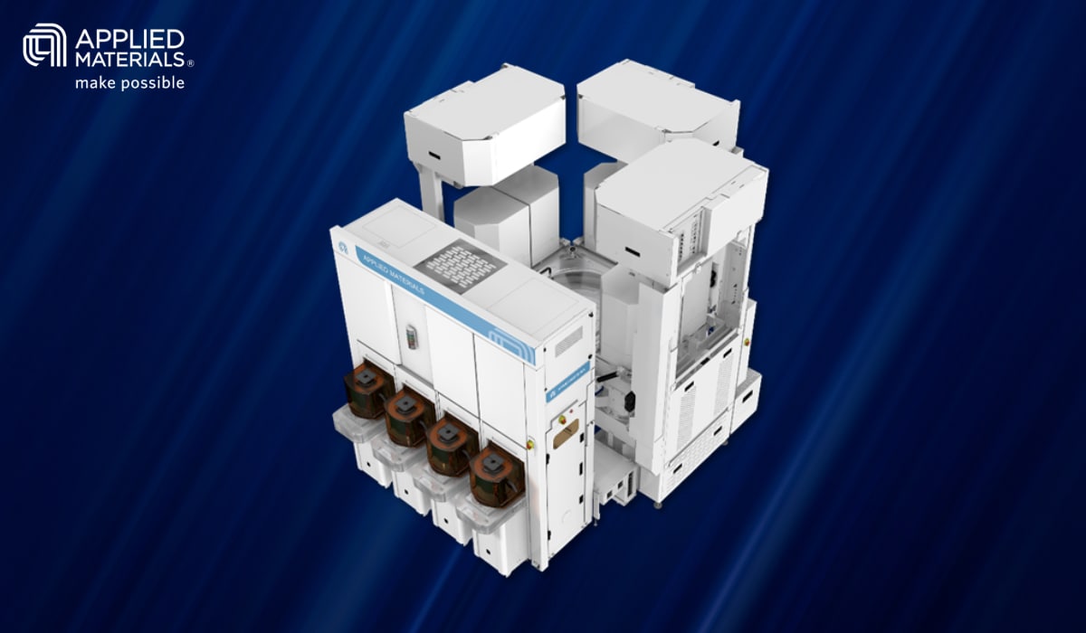
Applied Materials recently celebrated the shipment of our 10,000th CVD system. For more than 30 years, Applied has introduced a steady stream of product and material innovations that have transformed the CVD semiconductor equipment market. With our latest CVD product innovation, the Producer® XP Pioneer® CVD patterning film, we are positioned to enable the next generation of inflections in both memory and logic.

Applied Materials Earns Intel’s 2024 EPIC Distinguished Supplier Award
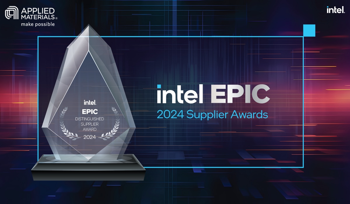
Applied Materials has earned Intel’s EPIC Distinguished Supplier Award. Through its dedication to Excellence, Partnership, Inclusion and Continuous (EPIC) quality improvement, Applied has achieved a level of performance that consistently exceeds Intel’s expectations.

Collaboration is Key to Enabling Advanced Patterning in the Angstrom Era
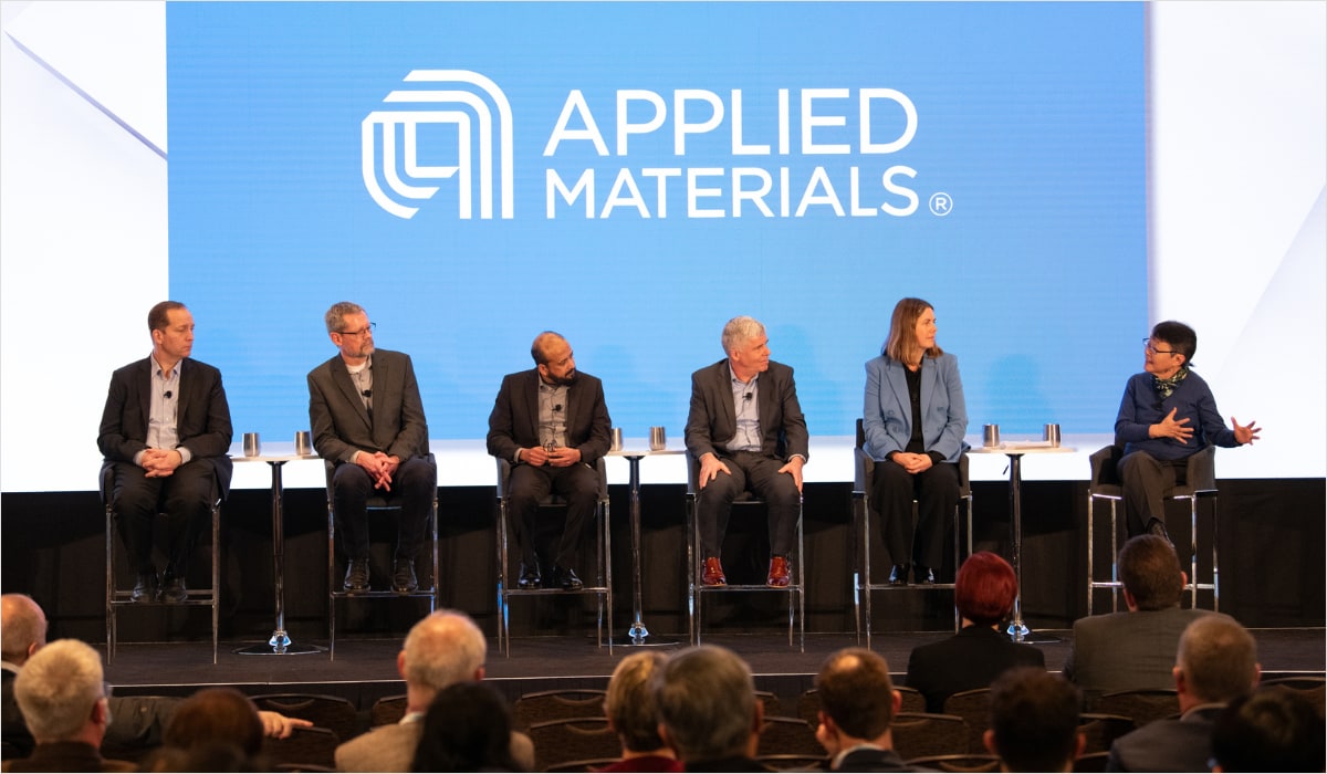
At the recent SPIE Advanced Lithography + Patterning Conference, Applied Materials hosted a panel titled, Patterning in the Angstrom Era: It Takes an Ecosystem, which delved deep into the changes coming to the patterning infrastructure across design, process and control.
