Products & Technologies
Products & Services
Contact
Products & Services
Products & Technologies
Services
Resources
Contact
Posted
February 21, 2024

Stay updated on our content.
Advanced Patterning in the Angstrom Era: Challenges and Opportunities
by Regina Freed
February 21, 2024
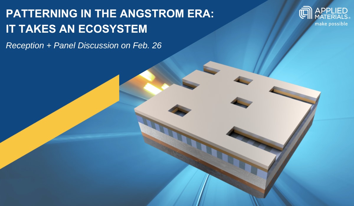
As leading chipmakers begin ramping process technologies at two nanometers and below, the industry is entering a new era where chip features will be described by a different unit of measurement – the angstrom, or one-tenth of a nanometer. Named after the Swedish physicist Anders Jonas Ångström, this unit is often used in the natural sciences to describe the size of individual molecules or biological structures. While there remains much debate about the actual meaning of semiconductor process node names, one thing is abundantly clear: the smallest dimensions are approaching the level of individual atoms.
New advances in lithography are required to pattern these unfathomably small features. EUV lithography has been in production for several years, and chipmakers have recently begun adopting EUV double patterning for the most critical layers. Next up on the roadmap is “High-NA” EUV, which promises to further boost our ability to shrink dimensions. While this lithography roadmap is well understood, many in the industry don’t realize that an entire ecosystem of adjacent capabilities is required to enable this advanced patterning – including software and design tools, materials engineering innovations in deposition and etch, and advanced metrology and inspection systems.
At the upcoming SPIE Advanced Lithography + Patterning conference in San Jose, CA, Applied Materials will bring together experts from across the chip design and patterning ecosystem to examine how we can overcome challenges presented by the next big inflections. Hosted by Applied and moderated by veteran industry reporter and editor Junko Yoshida, cofounder of the Ojo-Yoshida Report, the panel will feature leading technologists from NVIDIA, Intel, imec and Siemens EDA.
More details about the panel can be found on the Applied events page, including a link to register.
Angstrom Era Brings New Challenges and Opportunities for Innovation
I have the privilege of representing Applied on the panel, and I am excited to share my perspective on the opportunities presented by patterning in the “angstrom era,” which brings new challenges as patterning engineers implement progressively more complex EUV lithography approaches. For example, EUV lithography and photoresists are prone to “stochastic” effects that lead to random variations in the patterns transferred from the lithography tool to the photoresist. These variations can lead to a variety of defects, including line edge roughness and the formation of bridges in the space between metal lines, which can impact the performance of a chip or even cause a device to fail.
EUV patterns need to be transferred to the wafer with high fidelity. Etching quickly destroys the EUV photoresist, so a series of dielectric films are used as “transfer layers” that can withstand the etches. The transfer layers can become additional sources of variation that can lead to edge placement errors and other issues. EUV double patterning can help make tighter patterns, but it also introduces the risk of pattern registration errors that can create overlay issues and further edge placement errors. If detected prior to etching, edge placement errors require pattern rework, which wastes cost and time. If the errors are not detected, then manufacturers can experience yield loss or, perhaps worse, circuit variability that impacts chip performance and power consumption.
The transition to High-NA EUV lithography brings renewed scaling of line and space patterns, but it also introduces a new set of challenges. For example, High-NA optics reduce the exposure fields by one half. It therefore takes twice as many exposures to pattern a single wafer and can require complex reticle stitching to create larger chips such as AI processors. Additionally, chipmakers must evaluate several material changes, such as thinner resists and hardmasks to adjust for the changes in depth-of-focus, prior to deployment into volume production.
Thankfully our industry has a remarkable track record of overcoming challenges to keep the chipmaking roadmap moving forward. We have already seen many innovations developed across the full spectrum of ecosystem capabilities, from chip design methodologies and software modeling tools, to co-optimized adjacent process steps and enhanced metrology capabilities.
For example, at last year’s SPIE conference, Applied introduced the Centura® Sculpta® patterning system, which allows chipmakers to simplify EUV patterning schemes by elongating patterned features, bringing the tips of the features closer together than achievable with a single EUV or High-NA EUV exposure. Leading chipmakers are seeing excellent results as they deploy Sculpta systems in production and explore additional applications beyond EUV double patterning step reduction into pattern shaping for both EUV and High-NA EUV layers.
We will be sharing more news about Sculpta at the upcoming SPIE lithography conference, as well as highlighting new etch, deposition and metrology solutions to complement and improve chips made using EUV and High-NA EUV. These are just a few examples of the materials engineering innovations being developed by Applied in collaboration with our customers and partners. It truly takes an ecosystem to tackle the challenges of advanced semiconductor technology, and we’re looking forward to shining a spotlight on the new capabilities we’re introducing for the patterning engineer’s tool kit.
Regina Freed
Vice President, AIx™ Solutions

Regina Freed has more than 20 years of experience in the semiconductor industry, managing semiconductor process and equipment development for both logic and memory processes, including co-optimization between deposition and etch, lithography, metrology, and defect inspection. At Applied Materials, Regina leads our AIx™ program that enables us and our customers to accelerate development and ramp through Actionable Insights as well as control our processes to deliver improved process windows, enabling customers to scale faster and at lower cost, while optimizing device performance.
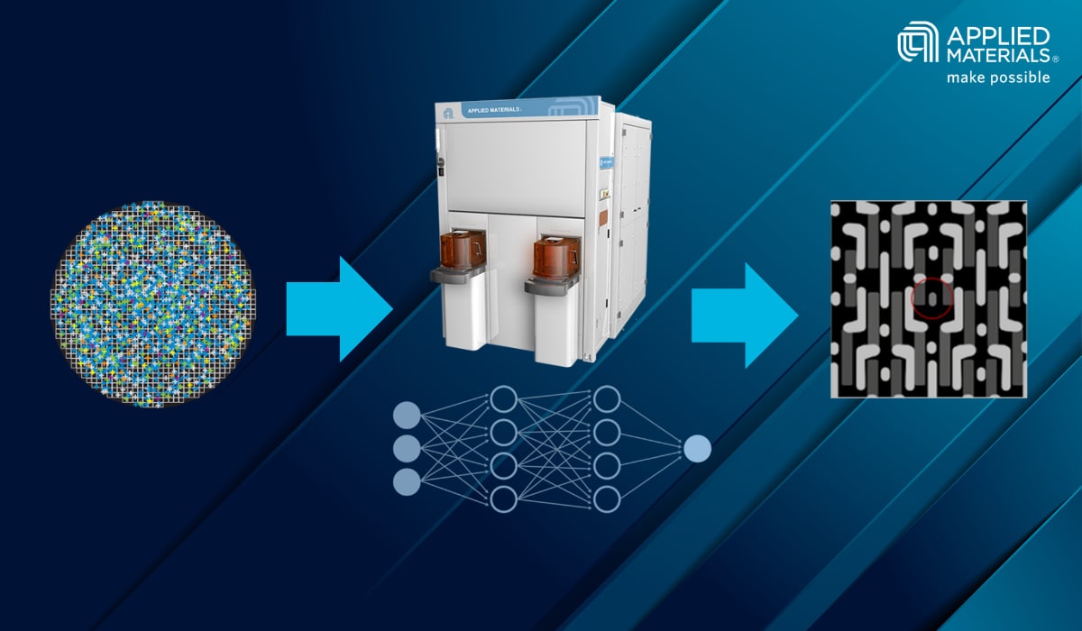
Separating the Signal from the Noise: Combining Advanced Imaging with AI for Chip Defect Review
As leading chipmakers begin ramping process technologies at two nanometers and below, the industry is entering a new era where chip features will be described by a different unit of measurement – the angstrom, or one-tenth of a nanometer.
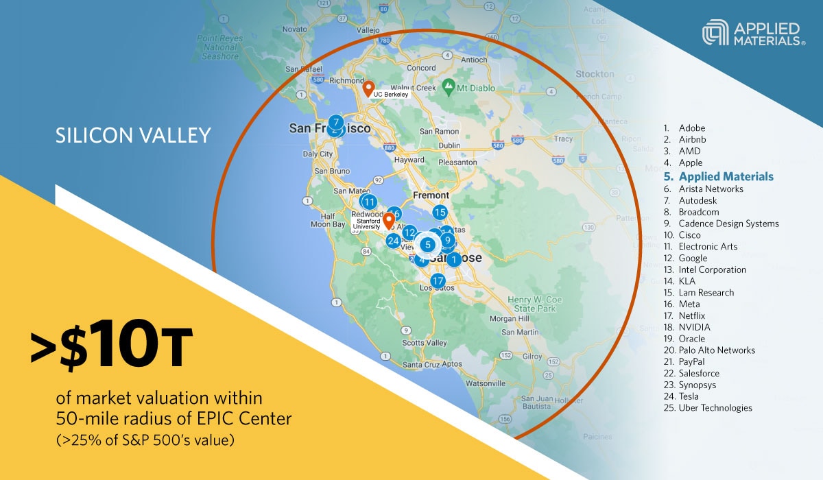
Why We’re Keeping the Silicon in Silicon Valley
In May 2023, Applied Materials announced our new Equipment and Process Innovation and Commercialization platform, the centerpiece of which will be the EPIC Center – a next-generation, multi-billion-dollar collaborative research facility located in Silicon Valley.

What’s Driving the Need for Innovation in ICAPS?
Applied Materials reached a significant milestone in 2023: For the first time, the largest portion of our wafer fab equipment sales came from customers in markets related to ICAPS – IoT, Communications, Automotive, Power and Sensors.