Products & Technologies
Products & Services
Contact
Products & Services
Products & Technologies
Services
Resources
Contact
Posted
November 09, 2021

Stay updated on our content.
Adding Sustainability to the Definition of Fab Performance

Nov 09, 2021
The semiconductor industry faces a significant challenge as it plans a major capacity expansion over the coming years. New fabs will need to produce greater numbers of increasingly complex chips built with more exacting processes—while also using less power and generating fewer emissions. Fortunately, Applied Materials’ engineers and scientists signed up for this challenge several years ago, and we are making more progress each quarter.
This is the second in a series of blog posts about how fabs are being conceived and equipped in new ways to promote a sustainable industry. In the previous post, my colleagues examined the support equipment that resides below the production floor in an area known as the sub-fab and explained how Applied’s iSystem™ can improve efficiencies, reduce emissions and lower energy consumption for chipmakers such as TSMC.
This post examines Applied’s efforts to drive fab sustainability through the process chambers, systems and software that we develop for chipmakers. More sustainable fabs will require new generations of equipment, and it all starts with an evolution in the mindset of how these systems are designed.
Defining “Performance” to Include Sustainability
Improving “Performance” is one of the most commonly expressed goals in chipmaking. Engineers focus on maximizing scorecard criteria including tool throughput, process uniformity and electrical characteristics, to name a few. Applied now includes sustainability on its performance scorecards and designs systems with a focus on minimizing:
- Energy consumption,
- The environmental impact of chemical use, and
- Footprint intensity, or the amount of cleanroom space needed per unit of wafers processed
In 2018, Applied created its Design for Sustainability Center of Excellence to help lead the semiconductor industry to identify cleaner, greener manufacturing methods. Using proprietary modeling tools, our experts develop power and emissions reductions strategies for process equipment during the design phase, well before the first piece of metal is cut to build a prototype. Creating digital models also enables new ideas to be applied to existing products already in the field. With these capabilities, we can model both the energy and chemical use in wafer processing in terms of equivalent CO2 emissions, enabling a real-world, holistic view of the impact of our reduction efforts.
In 2020 we upped the ante by announcing our “3 by 30” initiative for manufacturing systems. On a per-wafer basis, Applied is targeting a 30-percent reduction in equivalent energy consumption, environmental impact of chemical use and cleanroom area requirement—all by 2030.
Modeling Produces Insights
Calculating equipment energy needs encompasses many factors beyond just the direct electricity demands of the system. For instance, many systems need to be cooled with chilled water that is produced outside the cleanroom and pumped throughout the fab. That means energy savings can come from designing more thermally efficient systems to reduce the need for chilled water as well as improving the efficiency of chillers and heat exchangers. The SEMI organization’s S23 guidelines establish standards for this type of equivalent energy conversion in semiconductor manufacturing equipment. For example, the guidelines provide that every 1,000 liters of ultra-pure water usage is responsible for 9.0 kWh of energy needed to purify water to fab specifications, giving us a means to quantify the energy savings from reducing water use. Applied Materials has long had a voice in setting these industry standards. In fact, some of them were drafted by the engineering manager who recruited me to Applied.
Digital models of fab tools that include the equivalent energy demands of key components provide a more comprehensive view of the energy landscape of the fab and are invaluable in helping chipmakers identify how to reduce energy consumption effectively and without affecting other performance metrics.
Minimizing Chemical Impact
More efficient chemical use in semiconductor processing is a worthy goal, but deciding whether one chemical is more important to conserve than another is not always straightforward. To help address this issue Applied developed a framework for modeling the impact of our systems’ chemical use in relation to that chemical’s contribution to global warming.
Life Cycle Inventory (LCI) data that model CO2 emissions generated over a material’s production cycle (from raw material extraction through delivery to end-use location) is available for many chemicals our products commonly use. Even inert gases such as helium and argon, which are not greenhouse gases, have carbon emissions associated with their production and transport to a fab—which is sometimes called the “cradle-to-gate” footprint. For example, available LCI data from Sphera show that helium is about eight times more carbon intensive than an equivalent volume of argon. These insights help our engineers conceive greener recipes during process development.
Our framework also considers the emissions from our process chambers after abatement (or the “gate-to-grave” footprint). Detailed studies have quantified the Global Warming Potential (GWP) relative to CO2 of several greenhouse gases used in semiconductor manufacturing (see Figure 1).
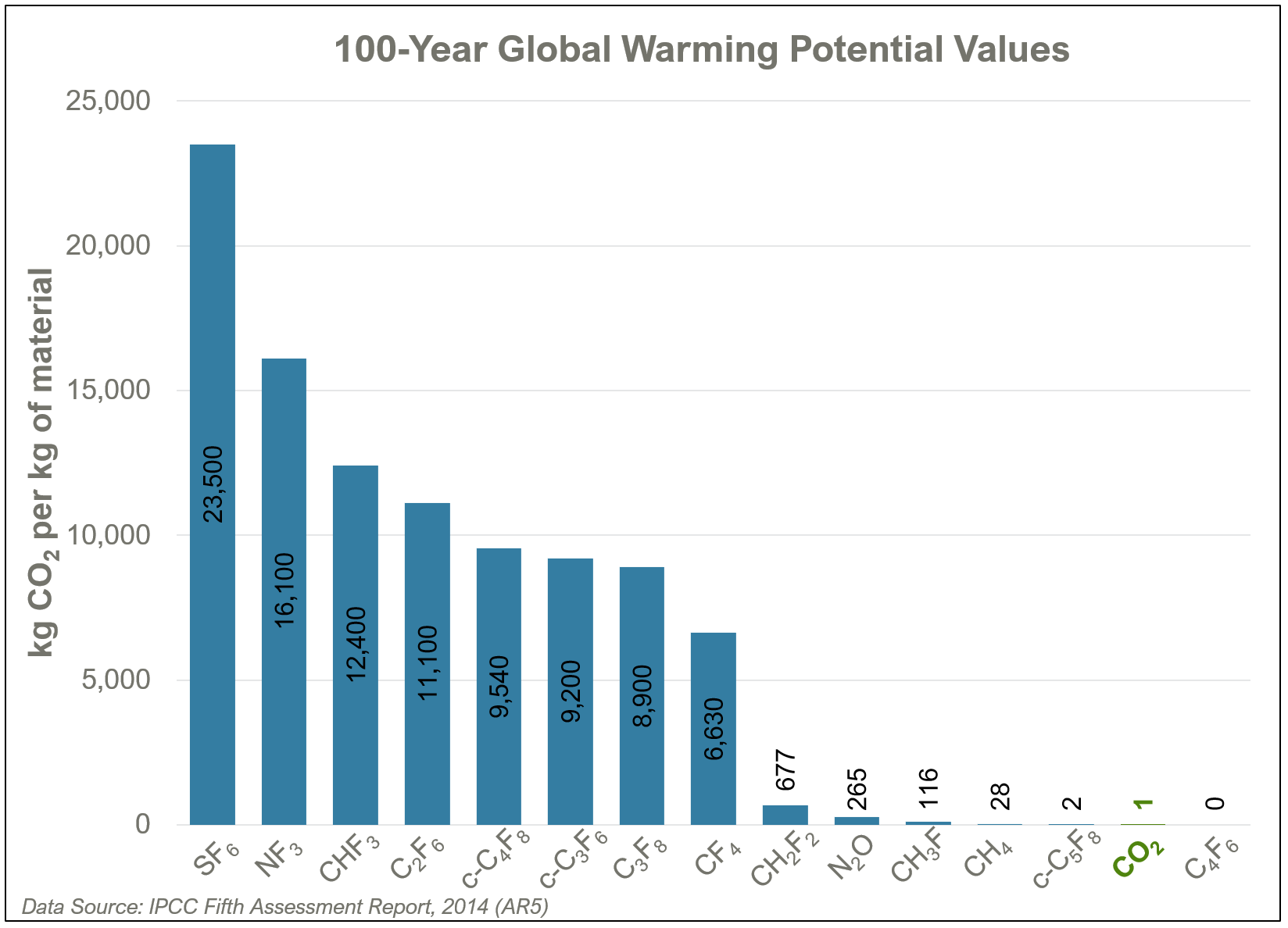
Figure 1: 100-year time horizon global warming potential for fluorocarbons and other greenhouse gases commonly used throughout the semiconductor industry, relative to CO2 by mass.
We combine these models to compose our cradle-to-grave view of chemical use (see Figure 2) and help to identify the best opportunities to reduce overall environmental impact. We share our analyses with customers so they can apply this knowledge in their own sustainability efforts.
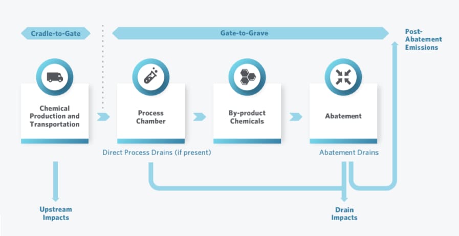
Figure 2: Cradle-to-grave envelope captures global warming impact from the production and transport of input chemicals, and wafer processing emissions following abatement.
Small is Big
Footprint is an important—but sometimes underappreciated—leverage point for improving fab sustainability. Simply put, a system with a smaller cleanroom footprint makes more efficient use of shared, energy-consuming resources such as air conditioning, piping and materials. Additional gains can be made by increasing the throughput of systems of a given footprint.
We are working on system designs for some of our major product categories that can deliver a 20-percent reduction in footprint per unit of wafers processed. These improvements will in turn help our customers meet their own sustainability goals, making each new wave of capacity expansion more eco-efficient.
It Takes an Industry
Creating a more sustainable semiconductor industry is a global, cooperative challenge, and the metrics used in our 3 by 30 initiative will guide Applied in making better design decisions for our chambers, systems and process technologies.
The global economy needs more semiconductors, and virtually every chipmaker has new fabs on the drawing board. We are committed to working with our customers and suppliers to drive greater sustainability in the fab, below the fab, and throughout the value chain upstream and downstream of Applied Materials. With the right mindset, together as an industry we really can Make Possible® a Better Future.
Check out our latest Sustainability Report to learn more about our efforts.
Tags: sustainability, fab efficiency, Environment, Design for Sustainability, 3 by 30, iSystem
Benjamin Gross, Ph.D.
Chemist and Systems Engineer, Design for Sustainability Center of Excellence

Dr. Gross is a Chemist and Systems Engineer with the Design for Sustainability Center of Excellence at Applied Materials, where he works in close partnership with the product engineering groups to reduce energy and chemical use in our process equipment. He supports Applied’s 3 x 30 initiative and is responsible for the metrics used to monitor progress toward our efficiency improvement goals. Ben has 14 years combined experience in strategic consulting and technical supply chain development. He holds a Ph.D. from Columbia University and a B.S. from the University of California at Berkeley, both in chemistry.
Innovations in eBeam Metrology Enable a New Playbook for Patterning Control
The patterning challenges of today’s most advanced logic and memory chips can be solved with a new playbook that takes the industry from optical target-based approximation to actual, on-device measurements; limited statistical sampling to massive, across-wafer sampling; and single-layer patterning control to integrative multi-layer control. Applied’s new PROVision® 3E system is designed to enable this new playbook.
Breakthrough in Metrology Needed for Patterning Advanced Logic and Memory Chips
As the semiconductor industry increasingly moves from simple 2D chip designs to complex 3D designs based on multipatterning and EUV, patterning control has reached an inflection point. The optical overlay tools and techniques the semiconductor industry traditionally used to reduce errors are simply not precise enough for today’s leading-edge logic and memory chips.

The Fourth Era of Computing Needs More than Advanced Logic and Memory Chips
At the Applied Materials Master Class today, we highlight two fast-growing and highly enabling areas of the semiconductor industry. “ICAPS” silicon powers billions of new devices on the edge—including electric vehicles. No longer an afterthought, packaging now enables the benefits associated with Moore’s Law to continue even as 2D scaling slows. Today’s class demonstrates that the AI Era requires innovation across a wide range of technologies, from the edge to the cloud.