Products & Technologies
Products & Services
Contact
Products & Services
Products & Technologies
Services
Resources
Contact
Posted
November 13, 2018

Stay updated on our content.
Accelerating New Materials Innovation through R&D Collaboration
Nov 13, 2018
Moore’s Law scaling is becoming challenged as emerging applications based on AI and big data require orders of magnitude improvements in chip performance and efficiency. Materials-enabled scaling including novel device architectures and new materials are needed to achieve these improvements.
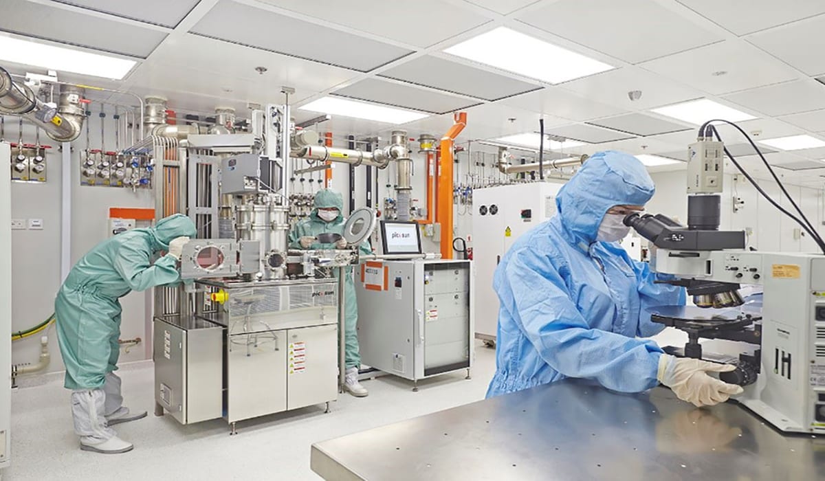
To augment and speed the pace of our R&D efforts in support of semiconductor roadmap advancements, Applied Materials and National University of Singapore (NUS) have established the Applied Materials-NUS Advanced Materials Corporate Lab. This is Applied’s first research lab jointly set up with a university in Singapore and its establishment is supported by the National Research Foundation Singapore (NRF). The goal of the lab is to accelerate discovery of new materials that can be quickly transferred into commercial applications for manufacturing future generations of semiconductors.
The new Applied Materials-NUS Advanced Materials Corporate Lab will offer world-class, multi-disciplinary R&D capabilities that span applied chemistry, materials science and microelectronics process engineering. Like Applied, NUS brings decades of experience in advanced materials research. The parties have identified new materials R&D and processing techniques with a focus on deposition and etching as two key research areas that will help pioneer innovative semiconductor structures and devices. Many researchers, engineers and graduate students with doctoral scholarships will come together in the lab to support their training and research in advanced materials.
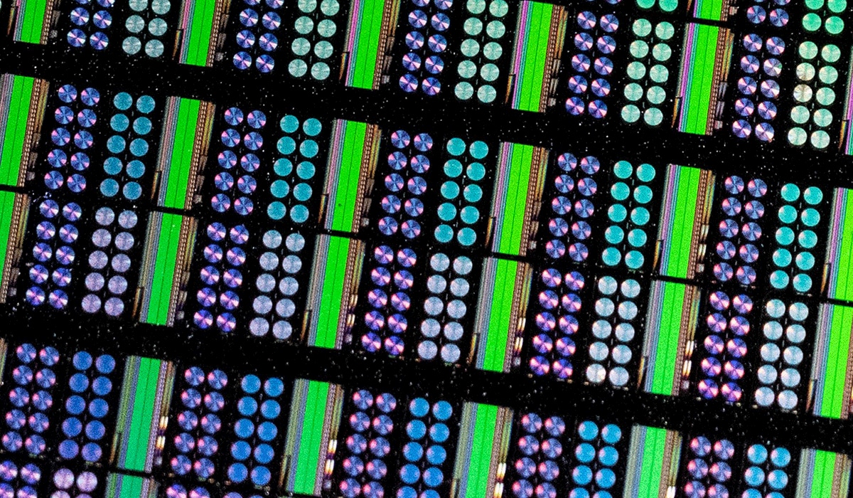
The work being done in this lab is important to the semiconductor industry because new materials are playing an increasingly critical role driving improvements in power, performance and area-cost (PPAC). Materials innovations have made possible lower leakage, higher speed transistors, lower delays in chip wiring and greater packing density. This has resulted in the evolution from mainframe to PC, then mobile and now to the emerging AI era, delivering enormous economic gains for society at each step.
Discovering and integrating new materials into the semiconductor manufacturing environment presents several challenges:
- The number of new materials used in semiconductor devices is expected to increase by 10x over the next decade. Materials for dielectrics, metals and multiple variants and combinations of the materials to deliver desired properties need to be developed.
- At the ultra-nanoscale level, materials behave differently than in a normal bulk state. Different laws of physics apply, dominated by surface forces over bulk properties. Materials are so small that surfaces and interfaces must be carefully engineered for the best performance.
- Today we see multiple thin nano-scale materials being stacked together in a single location to achieve desired properties; this means they must work together as a single entity. All this requires fundamental understanding and foundational research of new materials and their behavior at an atomic-level.
“Materials engineering has helped enable major advancements in semiconductors for decades, but never before has the need for new materials been greater than it is today,” said Dr. Prabu Raja, Senior Vice President of the Semiconductor Products Group at Applied Materials. “We are excited to launch the Applied Materials-NUS Advanced Materials Corporate Lab and look forward to a successful industry-academia collaboration. NUS and its focus on high-impact, multi-disciplinary science and engineering research make it a great institution to work with on new materials for next-generation semiconductors.”
NUS President Professor Tan Eng Chye said, “NUS is honored and privileged to be Applied Materials’ partner for its first university-based research laboratory in Singapore. The Applied Materials-NUS Advanced Materials Corporate Lab will draw on the complementary strengths of both organizations to address complex industry challenges. Successful projects completed under this Corporate Lab could potentially increase microelectronics-related activities in Singapore, and this in turn, could generate significant economic benefits for the country.”
Also commenting on the lab is NRF CEO Professor Low Teck Seng, “The semiconductor industry is highly competitive and manufacturers need to constantly innovate and upgrade their technology to stay relevant. Investing in R&D is therefore crucial for Singapore’s continued growth in the sector. The partnership between Applied Materials and NUS will introduce next-generation materials for manufacturing advanced semiconductors here. This is part of our strategy to strengthen innovation in the sector to meet the demands of the market through better products and training of our researchers.”
Singapore has a strong semiconductor ecosystem that extends from design to manufacturing, along with a successful track record of industry-academia partnerships. Applied values academic collaborations to understand critical technical issues and continues to expand its interaction with universities and institutes throughout the world. Applied Materials has operated in Singapore since 1991. Together with the government, we have established the Applied Packaging Development Centre, the Advanced Semiconductor R&D Joint Lab, and the SIMTech-Applied Materials Additive Manufacturing Collaboration.
From this important new collaboration with the NUS and the NRF, we can expand our ability to make discoveries that will drive technology innovation forward to support emerging applications.
Tags: NUS, R&D collaboration, materials engineering, National University of Singapore, NRF, National Research Foundation Singapore, advanced chips, Moore's Law
Applied Materials
Corporate Communications
The Applied Materials team publishes posts of general interest to our readers.
Now is the Time for Flat Optics
For many centuries, optical technologies have utilized the same principles and components to bend and manipulate light. Now, another strategy to control light—metasurface optics or flat optics—is moving out of academic labs and heading toward commercial viability.

Seeing a Bright Future for Flat Optics
We are at the beginning of a new technological era for the field of optics. To accelerate the commercialization of Flat Optics, a larger collaborative effort is needed to scale the technology and deliver its full benefits to a wide range of applications.
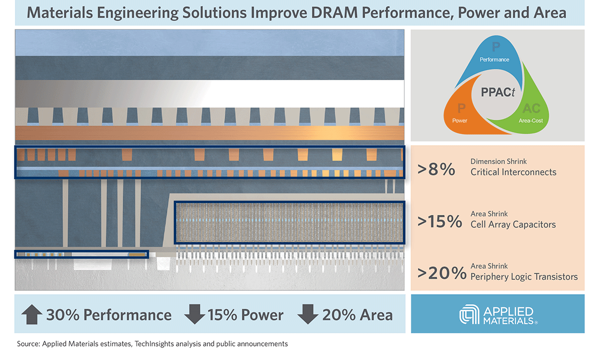
Introducing Breakthroughs in Materials Engineering for DRAM Scaling
To help the industry meet global demand for more affordable, high-performance memory, Applied Materials today introduced solutions that support three levers of DRAM scaling.