Products & Technologies
Products & Services
Contact
Products & Services
Products & Technologies
Services
Resources
Contact
Posted
October 09, 2019

Stay updated on our content.
A Quantum Future will be here Sooner than You Think

by Kenichi Ohno, Ph.D., Robert Visser, Ph.D. Nir Yahav
Oct 09, 2019
We often think quantum technology is a far-off future. Thanks to decades-long research on the elemental technologies and recent breakthroughs, the emergence of quantum may happen sooner than later. Large enterprises, start-ups, government agencies and research organizations around the world are investing billions of dollars to scale quantum technology from ideation to commercialization. As with any disruptive technology, the speed at which quantum can move from “lab to fab” will depend on the ability of the quantum ecosystem to work together to solve key technology challenges.
At Applied Materials, our open innovation approach includes convening key stakeholders and thought leaders around big industry inflections, like quantum, and issuing a rally call to all members across the value chain. Our recent Open Innovation Workshop brought together quantum technology leaders from Google, Harvard, IBM, Intel, MIT, Rigetti Computing, the University of Chicago, the venture capital community and select start-ups to identify key challenges in quantum information systems and explore opportunities for collaboration.
The central theme that emerged from the day is that quantum is about so much more than computing; there are many applications in areas like sensing, metrology and communications encryption on the near-term horizon. Today, quantum algorithms are solving practical problems in the fields of pharmaceuticals, finance, chemistry, manufacturing and cloud-based services. These applications do not require the level of precision and fault-tolerance as practical quantum computers; however, they do have complex challenges that need to be addressed now. In many cases, advancements in materials engineering can be a key part of the solution.
For example, when developing hardware for quantum applications, the number of gates on a chip is an important metric, but equally important is the error rate of each gate, which is directly connected to the materials quality. We learned about a figure of merit, termed “quantum volume,” which is defined as a multiple of the number of quantum gates and their error rate. Key capabilities from the semiconductor manufacturing industry, such as impurity control, scalable creation of tightly controlled devices and atomic-scale materials engineering, can potentially help improve quantum volume.
One speaker called for a “revolution” to change the current materials and interface device structures that superconductor-based quantum computing has relied on since the 1990s. Understanding the materials systems for quantum computing is complicated, so theoretical predictions can greatly help to design and fabricate those systems. Interestingly, the advancement of quantum computing technology in turn helps to make better quantum computers, because predicting materials used in quantum computing is one of the most compute-intensive calculations. As the industry starts to devise ways to integrate thousands to millions of quantum gates, supporting technologies including cryogenic equipment, RF electronics and high-throughput metrology need to be improved.
Another speaker emphasized the need for predictive creation and precise control of single quanta. He presented research demonstrating how semiconductor processing technologies can be used to fabricate devices for quantum transduction and quantum sensing. In the field of quantum optics, intriguing applications are emerging in secure communications. Some of the optical concepts can be used today in new types of AI learning circuits and to find new ways of solving problems at much lower energy consumption than conventional computers. A major challenge to commercialization is integrating complex optics on a chip. There are opportunities for semiconductor technology and materials engineering to play important roles in this space.
Experts from Applied Materials concluded the workshop by highlighting a variety of materials engineering capabilities enabled by the company’s state-of-the-art processing systems. These presentations showed what’s possible through materials modification at the atomic level, as part of a broader toolbox for engineers working on different aspects of quantum technology. As our CTO Om Nalamasu said, “Applied Materials wants to help reduce the time from invention to commercialization, and really make innovation and commercialization happen simultaneously.”
As quantum technology approaches the scale-up problem, we will need deeper collaboration throughout the ecosystem, including academic and government institutes. Applied Materials looks forward to bringing our capabilities in materials engineering and high-volume manufacturing to help accelerate the quantum future—from materials to systems.
Visit our collaboration site to learn more about Applied’s open innovation strategy and how we network with startups, research institutes, leading universities and more. You can also follow us on LinkedIn and Twitter to join our community of entrepreneurs, academics and industry partners building the next wave of emerging technologies.
Tags: Quantum Technology, Collaboration, Open Innovation Workshop, CTO
Kenichi Ohno, Ph.D.
Senior Process Engineer in the Advanced Technology Group

Dr. Kenichi Ohno is a senior process engineer in the Advanced Technology Group at Applied Materials, with a focus on process development for semiconductors and adjacent markets. He holds a Ph.D in materials science from the University of California, Santa Barbara, where he developed a materials synthesis technique for quantum sensing and processing, and a bachelor’s and a master’s degree in electrical engineering from the University of Tokyo, Japan.
Robert Visser, Ph.D.
VP of Engineering, Office of the CTO

Dr. Robert Visser is VP of Engineering in the Office of the CTO at Applied Materials. He is responsible for exploring business opportunities in new and adjacent markets related to advanced displays, optical components for augmented reality, ‘flat optics’ (metasurface based optics) and advanced packaging solutions enabling new packaging strategies for heterogenous integration. He also advises Applied's chemistry group in India at IIT Mumbai. With more than 30 years of industry experience, Dr. Visser has pioneered research and commercialization of display technologies related to thin film transistors, LCD materials, barrier films (including encapsulation materials), OLED and flexible displays. He holds a master’s degree in theoretical organic chemistry and physics, and a Ph.D. in physical and organic chemistry, both from Leiden University, Netherlands.

Nir Yahav
Now is the Time for Flat Optics
For many centuries, optical technologies have utilized the same principles and components to bend and manipulate light. Now, another strategy to control light—metasurface optics or flat optics—is moving out of academic labs and heading toward commercial viability.

Seeing a Bright Future for Flat Optics
We are at the beginning of a new technological era for the field of optics. To accelerate the commercialization of Flat Optics, a larger collaborative effort is needed to scale the technology and deliver its full benefits to a wide range of applications.
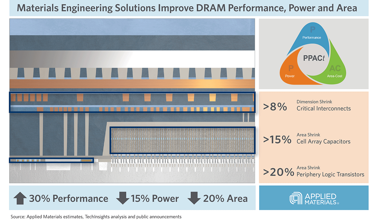
Introducing Breakthroughs in Materials Engineering for DRAM Scaling
To help the industry meet global demand for more affordable, high-performance memory, Applied Materials today introduced solutions that support three levers of DRAM scaling.