Products & Technologies
Products & Services
Contact
Products & Services
Products & Technologies
Services
Resources
Contact
Posted
June 30, 2023

Stay updated on our content.
A New Equipment Platform for a New Era of Chipmaking
by Mike Rice
June 30, 2023
Most semiconductor industry observers know it takes hundreds of process steps to make a chip. They can picture overhead transfer systems speeding orange FOUPs (Front Opening Universal Pods) full of wafers from tool to tool, imagining each process step being executed as quickly as physics allows before the wafers are zipped off to the next machine. They can sense the science behind the high-stakes race to produce the most precisely completed wafers in the shortest possible time.
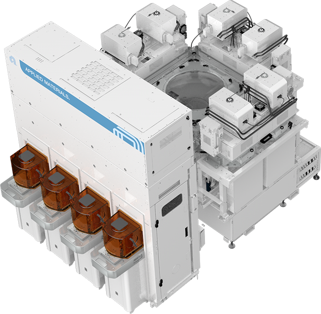
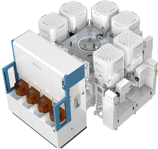
Fewer observers know that process tools are also a marvel of complexity. Each is based on a platform – a highly engineered set of modular components tailored for particular kinds of process chambers, steps and flows. The platform is painstakingly configured and tuned to achieve the best process step outcomes, which directly impact chip performance, power and yield. The platform can also be configured to accommodate differences in process step times: faster steps can be assigned a single chamber, while slower steps can be spread across multiple chambers. This load balancing helps all of the wafers in the FOUP to be processed in the shortest possible time and cost to help win the race.
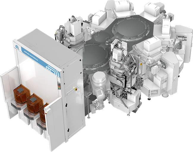
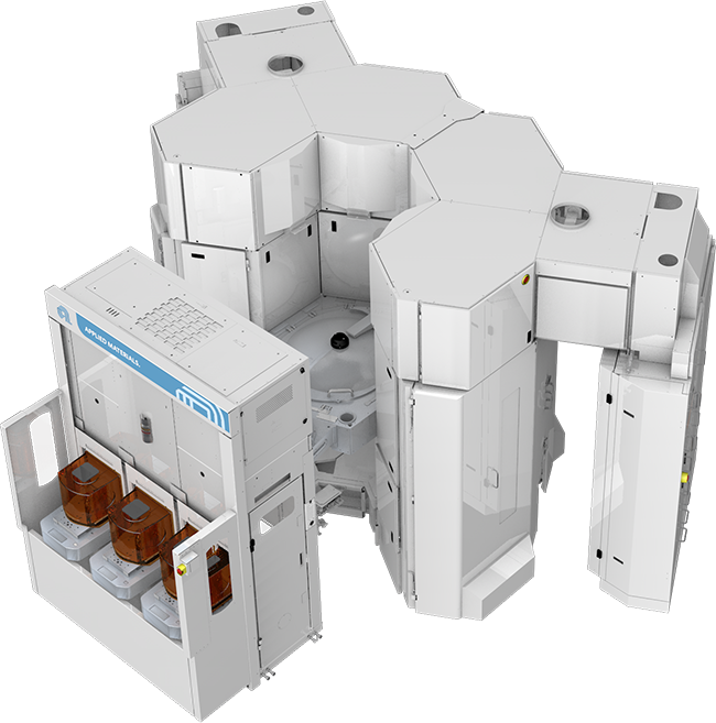
The platform is made up of a number of key components:
- A factory interface that receives FOUPs and wafers
- A central transfer chamber or mainframe, with one or more robots, that efficiently move wafers between locations
- One or more process chambers attached to the mainframe
- A suite of sensors that generates data about operating conditions
- Powerful real-time control computers and software tools that sequence, monitor and analyze operating conditions
The platform approach allows the system to be configured to the customer’s exact needs. Unit process systems are typically specialized to perform just one step – such as deposition or etch.
In co-optimized Applied Materials systems, consecutive steps such as deposition and etch occur in different systems, but are engineered by the company to deliver the best possible outcomes and performance when used together.
In Applied’s Integrated Materials Solutions, each platform is configured with a variety of chambers that perform a series of consecutive process steps in the same system, under high vacuum. This “factory within a factory” approach provides the highest possible level of cleanliness and control, while reducing transportation “queue times” that add time, risk contamination and increase variability between process steps.
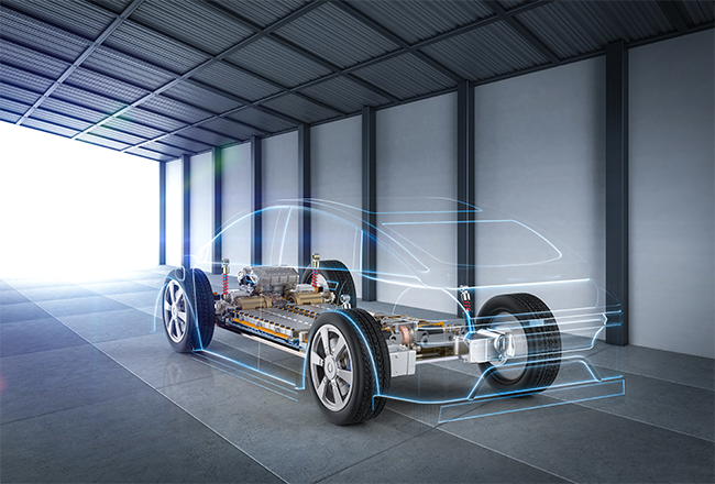
The platform approach is not unique to semiconductor manufacturing. It is frequently used in the auto industry, for example, where a common chassis and drivetrain can be configured with body designs tailored to different vehicle types, such as sedans, small SUVs and passenger vans.
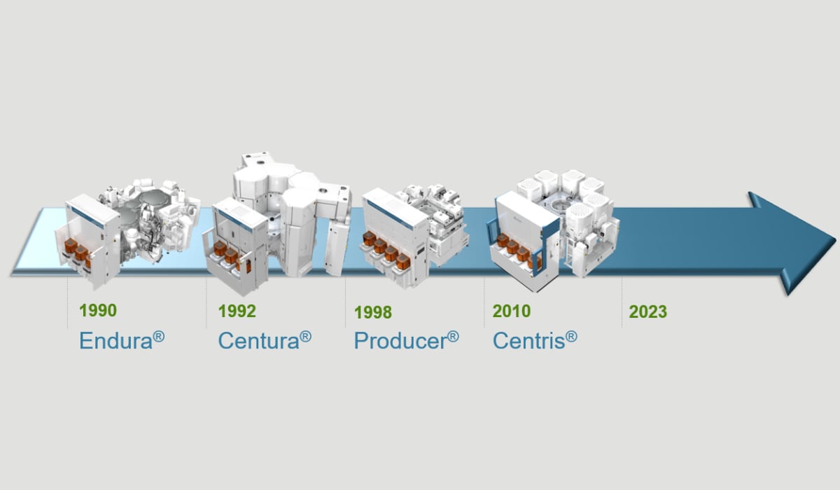
A Legacy of Leadership Platforms
Applied Materials has the world’s largest installed base of around 45,000 wafer manufacturing systems. We ship thousands of new systems each year, and most are based on just four major platforms that were introduced and refined over the past three decades. Just as automakers develop different platforms for passenger vehicles, light trucks and large commercial vehicles, each of Applied’s major platforms enables chipmakers optimize their fabs for particular wafer processing needs and workloads.
Applied Endura®
Launched in 1990, the Endura® platform is one of the most widely adopted deposition systems in the industry. The platform’s staged, ultra-high-vacuum architecture delivers extreme film purity. With its unique ability to integrate multiple process technologies on a single platform, the Endura platform has been chosen to host major innovations in process integration including high-k metal gate transistors, selective tungsten transistor contacts, and a copper barrier seed solution that integrates 7 consecutive process steps to cut interconnect resistance in half.
Applied Centura®
Introduced in 1992, the Centura® platform incorporates the high-vacuum capabilities pioneered by Endura along with advanced robotics that increase throughput. The Centura platform is designed with larger facet sizes that support the bigger chambers used in etch, epitaxy, and HDP CVD for example.
Applied Producer®
Launched in 1998, the Producer® platform is designed to perform individual process steps at the highest speed, smallest footprint and lowest operating cost. This solution continues to be an industry workhorse for CVD as well as selective etch and treatment technologies. Producer is used in all semiconductor markets, including high-k metal gate and FinFET transistors along with 3D NAND memories.
Applied Centris®
The Centris® platform was introduced in 2010 with the goal of being the smartest and fastest platform for conductor etch applications in memory and logic. Centris included an unprecedented eight process chambers – six for etching and two for plasma cleaning. The compact system increased throughput to 180 wafers per hour and cut production costs by up to 30%. In 2015, Centris became the platform for Applied’s Sym3® etch system, the fastest ramping product in company history.
These four platforms are all still going strong and will continue to play a vital role in furthering our customers’ technology roadmaps.
New Challenges Call for a New Platform
The semiconductor industry faces a new set of challenges. With traditional 2D scaling slowing in recent years, the industry is increasingly relying on a “new playbook for PPACT” – performance, power, area-cost and time-to-market. The new playbook consists of:
- New architectures – including GPUs and TPUs that accelerate AI workloads
- New materials – like pure tungsten transistor contacts that lower wiring resistance
- New 3D structures – such as gate-all-around transistors and backside power delivery networks
- New ways to shrink – including Sculpta™ pattern-shaping technology that reduces EUV double-patterning steps
- And heterogeneous integration – which enables chip designs to be partitioned into chiplets that can be recombined for improved performance, power and cost
Flexibility
Platform innovations will be needed to drive the new playbook. In particular, the new architectures for AI rely on new materials and 3D structures that will be common in the angstrom nodes. There will be a greater need for integrated materials solutions that allow increasingly delicate materials and structures to be created and combined in high vacuum. The ideal platform will enable chipmakers to integrate more process chambers – including significantly different process technologies or architectures – and accommodate more steps than ever before, all in a single flexible, high-throughput system.
Intelligence
The complexity of emerging process recipes is exploding. While unit processes like etch require engineers to optimize as many as 100 different process variables, integrated materials solutions dramatically increase the number of variables and challenge even the most experienced process integration experts. Increasingly, progress depends on sensors, massive data generation and analytical tools that help engineers create sophisticated recipes that result in the best chip performance and power characteristics together with the widest acceptable process margin or “window.” The ideal platform will gather as much actionable data as possible for process engineers and their analytical tools. A more intelligent platform will also help chipmakers maximize productivity across all stages of the process lifecycle, from R&D to ramp and high-volume manufacturing.
Sustainability
The increase in process complexity and steps will add to the challenge of creating a more sustainable semiconductor industry. Without significant innovations, electricity and materials consumption per wafer will continue to increase, and the carbon emissions will grow correspondingly. A more sustainable platform will help reduce the industry’s emissions per wafer.
Applied’s platform design team has been monitoring these trends over the past several years and imagining a new equipment platform for a new era of chipmaking. I look forward to sharing more details at our SEMICON West Technology Breakfast on the morning of July 11 in San Francisco. I hope to see you there!
Mike Rice
Corporate Vice President, Engineering - Semiconductor Products Group

Mike Rice is Corporate Vice President of Engineering in the Semiconductor Products Group. He is responsible for leading and developing core competencies and product solutions to support company growth and partnering with suppliers to deliver high-quality products. In July 2011, he was awarded the honorary designation of Applied Materials Fellow for his outstanding technical contributions that have been vital to the company’s success. Mike joined Applied Materials in 1992 as an engineering manager in dielectric etch and has served in roles with increasing responsibility across etch and foundation engineering. His broad capability and wealth of engineering experience has been invaluable in the development and performance of common and automation subsystems used across all of Applied’s product lines.
Mike earned a bachelor of science degree in mechanical engineering from California Polytechnic State University in San Luis Obispo. He holds more than 180 patents in plasma etching, ALD products, robotics, mainframes and platform architectures.

Doubling Down on Collaboration at SEMICON West 2023
The semiconductor industry has proven itself more than capable of achieving growth by collaborating to overcome big challenges. Collectively, we have demonstrated innovation and resiliency that is fueling what several industry analyst firms project will be a $1 trillion semiconductor market by 2030 that could directly seed $3-4 trillion of global electronics growth.
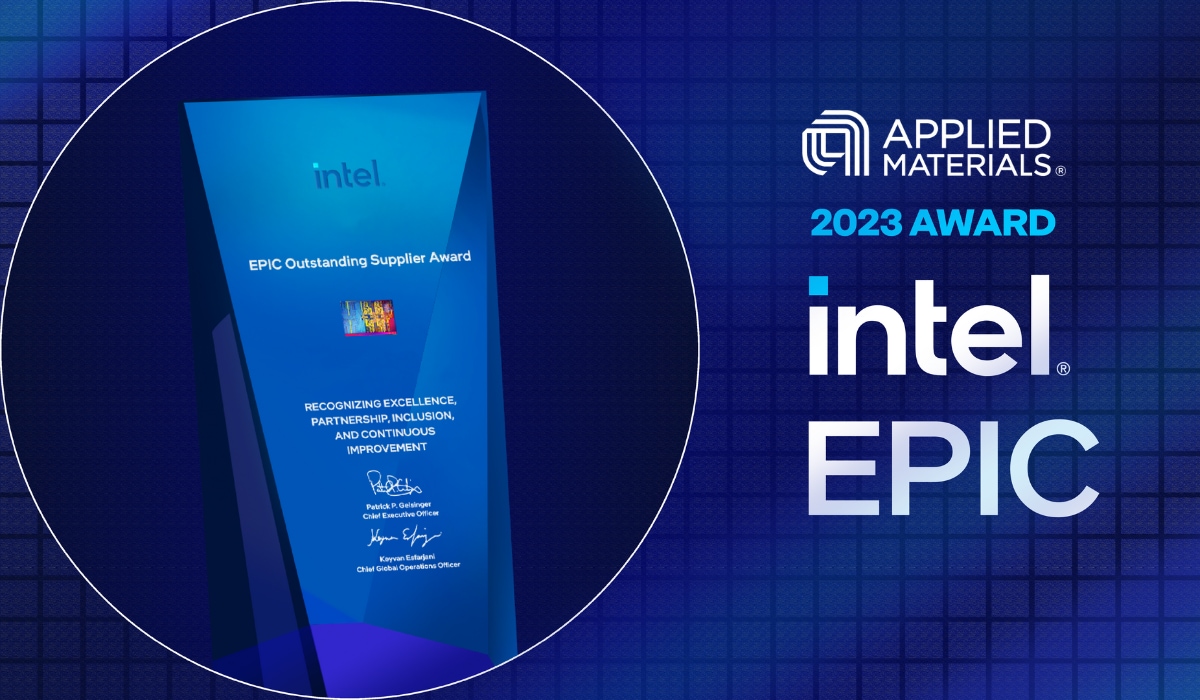
Applied Materials Earns Intel’s 2023 EPIC Outstanding Supplier Award with Supplier Diversity Distinction
Applied Materials has earned the exclusive Intel EPIC Program Outstanding Supplier Award with Supplier Diversity Distinction for 2023. This award recognizes the absolute top performers in the Intel supply chain for their dedication to continuous quality improvement, performance, collaboration and inclusion over the past year.
As Chipmakers Assess “Where” to Build New Fabs, the “How” of Semiconductor Innovation Must Remain a Priority
According to Ericsson, there are more than 6.5 billion smartphone users worldwide. I would speculate that very few of them have ever given much thought to what’s inside that phone — a miracle of science, engineering and manufacturing that is arguably one of humankind’s greatest technical accomplishments.