Products & Technologies
Products & Technologies
Services
Resources
Posted
December 19, 2023

Stay updated on our content.
10,000 Chambers and Counting: Celebrating the Centris® Sym3® Etch System

by Somit Joshi
December 19, 2023
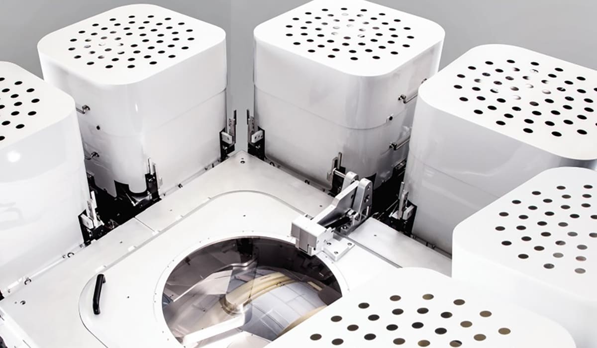
As we close the year at Applied Materials, we are celebrating a major milestone. Recently, we marked the shipment of our 10,000th Centris® Sym3® etch chamber. The Sym3 product family is Applied’s most advanced etch system, using innovative technologies to provide extremely high materials selectivity and profile control. This system enables our customers to create densely packed, high-aspect-ratio structures across memory and logic applications, including emerging architectures such as gate-all-around (GAA) transistors.
Introduced in 2015, the Sym3 system represented a brand-new design concept in the industry, built from the ground up to solve persistent and impending industry challenges. The etch chamber was the first to feature Applied's True SymmetryTM technology, with a fully symmetrical architecture across the three key etch process parameters of flow rate, temperature and power (RF). This unique architecture provided multiple tuning controls for optimizing process uniformity to the atomic level.
The Sym3 family quickly became the fastest ramping product in Applied’s history, reaching 5,000 units shipped in 2020, just five years after launch. Remarkably, it only took three years to ship the next 5,000 chambers – a testament to the strong pull from chipmakers.
As traditional 2D scaling has slowed, Sym3 has given chipmakers new ways to continue innovating by precisely shaping materials to generate 3D structures, such as those used in GAA transistors and 3D NAND channel hole patterning. An enabler for this unique capability is the industry-leading high-conductance chamber architecture that provides exceptional etch profile control by quickly and efficiently exhausting the etch byproducts during the process sequence.
The addition of the Sym3 Y chamber in 2020 strengthened this highly successful product family by allowing chipmakers to shape ever-smaller features in leading-edge memory and logic chips. By introducing a new proprietary coating that protects critical chamber components during the etch process, we have enabled chipmakers to reduce manufacturing defects and improve wafer yield. Further, by co-optimizing the Sym3 system with unique chemical vapor deposition (CVD) patterning films, customers can increase the layers in 3D NAND memory devices and reduce the number of steps needed in the quadruple patterning of DRAM layers.
To address the growing requirements of transistor and memory scaling, we have continuously designed in additional improvements since Sym3 was first introduced, including advanced pulsing schemes, higher-conductance chambers, and very-high and very-low temperature process regimes.
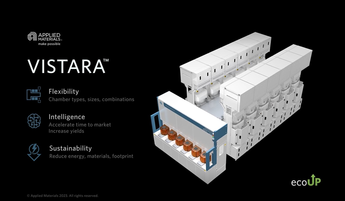
Additionally, we recently released the VistaraTM platform, which further extends the productivity of the Sym3 etch technology by enabling higher chamber density. With Vistara, we will have the flexibility to cluster more than just one application, combined with sensors/AI to enable process optimization and the latest sustainability solutions to help reduce the industry’s emissions per wafer.
Looking ahead, we are continuing to evolve the Sym3 platform to address the etch challenges of emerging technology inflections:
- Foundry/Logic: The GAA transistor architecture requires minimal depth variability and perfectly vertical profiles across a wide array of nanosheet widths.
- DRAM: Memory stacking requires extremely small spaces (<10nm) with very tight profile control.
- NAND: High-aspect-ratio etches are required to extend the roadmap to 300 stacked layers and beyond.
With unmatched process uniformity and defect control, the Sym3 system offers customers new ways to shape and pattern materials as chip features become tighter and smaller, aspect ratios increase, and materials engineering grows more complex at advanced nodes.
Somit Joshi
Managing Director of Marketing, Etch

Somit heads the Strategy & Product Management team in Applied’s Etch business unit, where he is responsible for driving the product strategy and strategic planning for upcoming industry inflections. Somit has more than 25 years of experience in the semiconductor industry across both device makers and OEM providers. He holds an MBA in product management and an MS in materials science.

Enlight® 2: Accelerating Brightfield Optical Inspection in a New Era of Chipmaking
In 2021, Applied launched the Enlight® brightfield optical wafer inspection system, which combines industry-leading speed with high-resolution optics that capture more yield-critical data from each wafer scan. Today, Applied is introducing Enlight 2 – an upgraded system that brings new levels of throughput and sensitivity to help chipmakers detect the highest number of yield-killing defects while maintaining low false-alarm rates.

A Deeper Look into the Vistara Platform
At SEMICON West 2023, Applied Materials introduced its most significant new wafer manufacturing platform in more than a decade. Designed to be a trusted solution for many years of customer innovation and productivity, the Vistara platform is architected based on three pillars: flexibility, intelligence and sustainability. A newly released animation video brings to life the capabilities and components behind each of these pillars.
A New Equipment Platform for a New Era of Chipmaking
Most semiconductor industry observers know it takes hundreds of process steps to make a chip. They can picture overhead transfer systems speeding orange FOUPs (Front Opening Universal Pods) full of wafers from tool to tool, imagining each process step being executed as quickly as physics allows before the wafers are zipped off to the next machine. They can sense the science behind the high-stakes race to produce the most precisely completed wafers in the shortest possible time.
