Products & Technologies
Products & Services
Company
Contact
Products & Services
Products & Technologies
Services
Resources
Company
Contact
Semiconductor
Patterning
Technologies
Software
Photomask
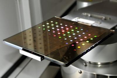
A photomask contains the pattern of an integrated circuit. And as transistors have become smaller and smaller, photomasks have become more complex to accurately transfer the pattern to silicon wafers. The process of creating photomasks has become correspondingly more advanced—even slight defects in a photomask can impact silicon device performance. Verifying that the photomask pattern is accurate and defect-free is critical, especially in the case of high-revenue-earning chips.
A photomask is a fused silica (quartz) plate, typically 6 inches (~152mm) square, covered with a pattern of opaque, transparent, and phase-shifting areas that are projected onto wafers in the lithography process to define the layout of one layer of an integrated circuit. Numerous successive patterns guide deposition or removal of material from the wafer in subsequent patterning steps (click here to read more about patterning).
Photomask is an expanding segment for Applied; in response to the growing demand for photomasks for volume production of mobile, automotive, and Internet of Things applications, its systems address a significant part of the photomask manufacturing flow.