Products & Technologies
Products & Services
Company
Contact
Products & Services
Products & Technologies
Services
Resources
Company
Contact
Semiconductor
Patterning
Technologies
Software
Metrology and Inspection
In addition to metrology and wafer inspection, defect review, analysis, and classification are vital as the means to monitor and control the quality of individual steps in the semiconductor manufacturing sequence. Metrological procedures verify that target physical and electrical properties of the devices under production are being met at every step, while wafer inspection identifies surface particles, pattern flaws, and other conditions that may compromise performance of the completed device.
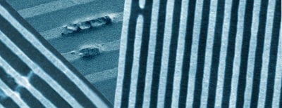
Applied offers a full suite of metrology, inspection, and review systems for FEOL and BEOL applications. These systems’ optical capabilities and algorithms meet the most advanced technical demands, such as SADP and SAQP, extreme ultraviolet layers, measurement-intensive optimal proximity correction mask qualification, and emerging 3D architectures that make complete and accurate imaging more challenging. Their leading-edge capabilities enable chipmakers to establish accurate statistical process control, ramp up production runs rapidly, and achieve consistently high production yields.