Products & Technologies
Products & Services
Company
Contact
Products & Services
Products & Technologies
Services
Resources
Company
Contact
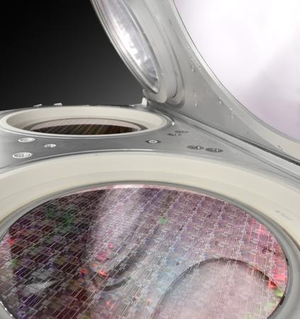
Semiconductor
Patterning
Technologies
Software
CVD
CVD is a process in which a substrate is exposed to one or more volatile precursors that react or decompose on the substrate surface to produce the desired thin film deposit. CVD processes are used for a broad spectrum of applications. These range from patterning films to insulation materials in transistor structures and between the layers of conducting metal that form the electrical circuit (e.g., STI, PMD, IMD, conformal liner and conductor gap fill).
CVD processes are also important in strain engineering that uses compressive or tensile stress films to enhance transistor performance through improved conductivity. Applied’s diverse solutions meet critical demands for void-free gap fill in complex topography with demanding feature profiles, progressively lower-capacitance materials that help boost transistor speeds, and robustness to withstand additional process steps accompanying WLP techniques being adopted for advanced mobile technologies.