Products & Technologies
Products & Services
Contact
Products & Services
Products & Technologies
Services
Resources
Contact
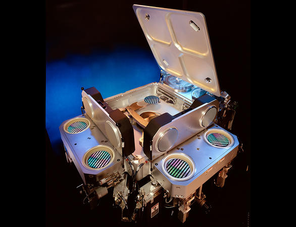
Producer® CVD
CVD technologies are essential for semiconductor processing and a necessary component to all semiconductor devices from logic, DRAM, and NAND to MtM market segments such as MEMS, photonics, IoT, and power device technologies. The Applied Producer platform has served as the foundation for the development of a wide range of films, each with its own unique set of process requirements to be deposited on an equally wide range of structural geometries (blanket, gapfill, conformal).
Introduced in 1998, the Producer platform for 150mm, 200mm, and 300mm wafers stands as one of the most successful platforms of all times, spanning key technology inflections for 10 nodes. Its innovative Twin Chamber® architecture enables simultaneous processing of up to six wafers for superior productivity. With ceramic heaters and chamber components and a remote plasma source for chamber cleans, the Producer delivers the lowest defectivity for CVD films. The platform can handle a variety of MtM substrates (including SiC wafers) reliably and carefully from loadlock wafer mapping to clear wafer orientation to wafer placement.
Enabling traditional PECVD (TEOS and silane-based oxides and nitrides) and sub-atmospheric CVD films, the Producer system accommodates low-k, strain engineered, litho-enabling films, thermal films, high-temperature PECVD applications, SiGe, and a-Si. Some examples of its capabilities for MtM device applications are thicker films (≥20µm), lower-temperature processes (180°-350°C), more conformal films, and new materials such as low-temperature PECVD silicon germanium (<50um) and a-Si.
Platform extendibility enables customers to leverage the Producer toolset for multiple device types and process nodes.