Products & Technologies
Products & Services
Contact
Products & Services
Products & Technologies
Services
Resources
Contact
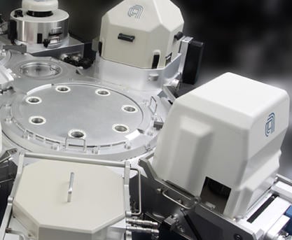
Endura® iLB™ PVD/ALD
The Applied Endura iLB PVD/ALD system with Centinel® chambers answers the challenge of growing contact resistance as dimensions shrink and the integrated liner/barrier (iLB) thickness consumes a greater percentage of tungsten plug volume.
The system offers a cost-effective way of using ALD (atomic layer deposition) technology to extend customers' existing iLB PVD/CVD installed base to 32nm and beyond by delivering >90% coverage of ultra-thin, uniform, high-quality barrier film. It deposits TiN films with minimal risk of plasma damage or adverse changes in high-k material properties, thereby enabling advanced memory applications.
The Centinel technology enhances the Endura iLB integrated PVD/CVD (physical vapor deposition/chemical vapor deposition) process platform with the RE-ALD (radical-enhanced atomic layer deposition) chamber that enables optimized tungsten volume with resultant lower contact resistance in ≤32nm logic devices. It is also intended for 4X node embedded DRAM, DRAM electrode, and buried word line applications.
The excellent step coverage achieved with the Centinel process makes it possible to minimize the barrier thickness needed to optimize deposition uniformity inside features. Besides maximizing the volume available for tungsten fill, the extreme thinness of the barrier layer reduces the time required to process each wafer and contributes to high productivity. As no backside deposition occurs, productivity is not adversely affected by back-side cleaning. Another benefit is the lower processing temperatures at which the chamber operates, thereby avoiding recrystalization damage to high-k materials.