
製品・サービス
製品・サービス
半導体
市場と変化
ソリューションとソフトウェア
VeritySEM 20 臨界寸法(CD)計測
半導体デバイスのパターン測定に関して言えば、CD-SEM(臨界寸法走査型電子顕微鏡)は、最も精密なサブナノメートルレベルの測定値を生成し、その計測データをリソグラフィスキャナに供給することで制御するため、「ファブの定規」と呼ばれることが多い。CD-SEMは、リソグラフィスキャナがマスクからフォトレジストにパターンを転写した後、線や間隔などのパターンの重要な寸法を測定するために使用されます。この計測値に基づき継続的にリソグラフィとプロセスをキャリブレーションすることで、確実に補正されたパターンがウェーハにエッチングされます。EUV、特に高NA EUVの採用によりフォトレジストはさらに薄くなり、デバイスフィーチャーの微細寸法の計測はますます困難になっています。深紫外光に比べて利用できる光子数が10分の1しかないため、マスクパターンを形成するには、より薄いフォトレジストが必要となる。レジスト層を薄くすることで、EUV露光で形成された高密度なラインが互いに崩壊するのを防ぐ効果もある。高NAに移行すると、高NA EUVスキャナの焦点深度の低下を補うために、レジストはさらに薄くなる。
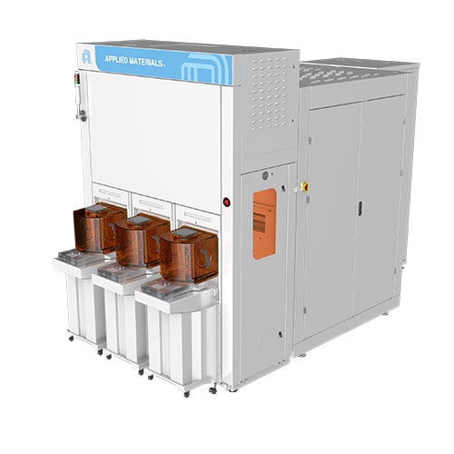
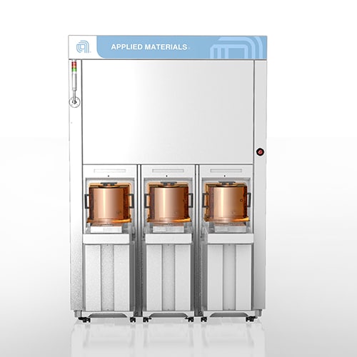
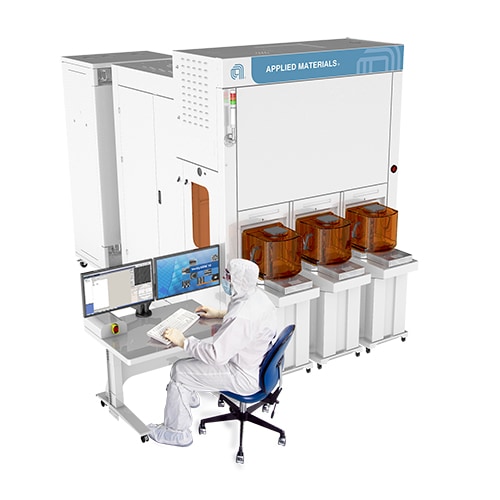
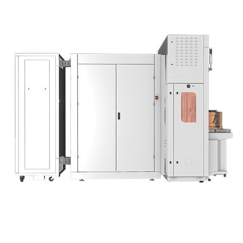
Applied VeritySEM™ 20 CD-SEM計測プラットフォームは、高度なロジックおよびメモリの重要な寸法を測定するために特別に設計されています。このシステムは、業界をリードするサブナノメートル級の電子ビーム解像度を用いて、ウェハー全体にわたる数百もの高精度なCD測定値を迅速に取得します。業界をリードする解像度とスキャン速度により、EUVスキャナのキャリブレーションが高速化され、顧客はプロセスレシピの開発を加速し、量産における歩留まりを最大化し、大型リソグラフィモジュールへの投資に対するROIを高めることができます。低い入射エネルギーは、EUVおよび高NA EUVのより薄く繊細なフォトレジストとの相互作用を最小限に抑え、パターンの忠実度を維持しながら、厳しい計測生産要件を満たします。
VeritySEM 20は、ゲートオールアラウンド(GAA)トランジスタ、DRAM、および3D NANDメモリの計測機能を強化しています。多方向走査方式により、EUVおよび高NA EUV層用の超薄型レジストのエッジ形状の安定化とエッジ対称性の向上が可能になります。同時に、用途に応じて20~50%のスループット向上を実現するとともに、2D構造におけるマッチング精度を最大25%向上させます。VeritySEM 20は、改良されたチャンバー汚染制御機能を搭載しており、汚染のない計測を可能にすることで、長期にわたる安定したスキャナ校正を実現します。直感的なレシピ作成フローを備えた新しいインフラストラクチャは、レシピ作成時間の短縮とユーザーの生産性向上を目的として設計されています。また、AIベースの測定最適化により、レシピの堅牢性が向上し、ユーザー間のばらつきが低減され、顧客はより短時間で決定的なレシピパラメータに到達できるようになります。
VeritySEMは、BSEイメージング技術のパイオニアであり、現在大量生産で利用可能なSEMカラムの中で最高解像度を誇ります。
- 1 / 4
- 2 / 4
- 3 / 4
- 4 / 4