Products & Technologies
Products & Services
Company
Contact
Products & Services
Products & Technologies
Services
Resources
Company
Contact
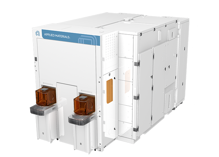
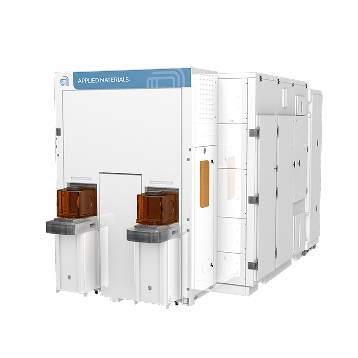
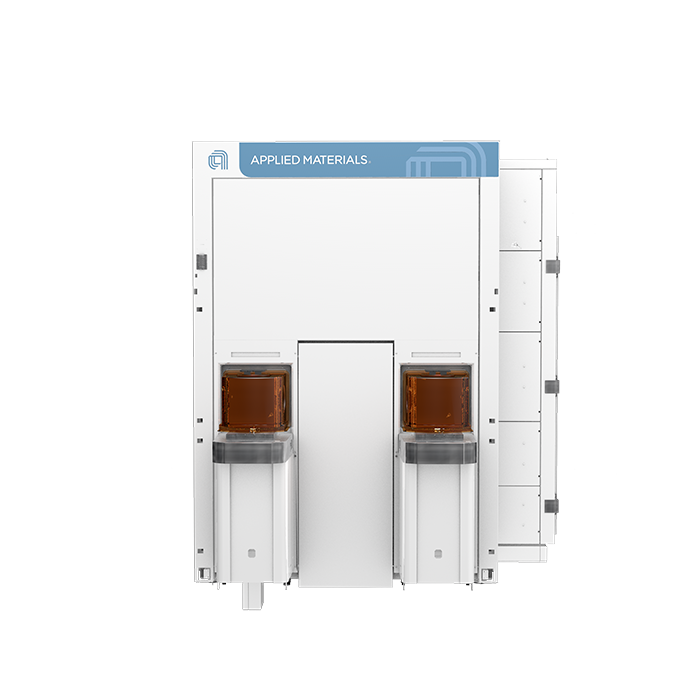
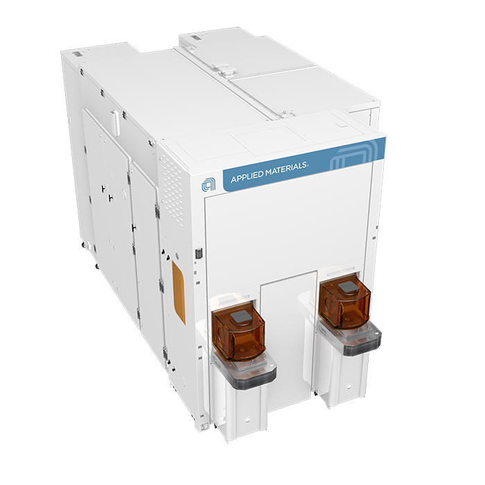
PrimeVision® 10 eBeam Inspection
As semiconductor devices and architectures continue to grow in complexity and vertical scale, defectivity reduction and control become even greater challenges when trying to speed up time-to-market. Fabrication processes continue to add more steps with ever tightening process windows, requiring higher sensitivity in 2D and 3D imaging. Identifying the most yield-critical defects becomes extremely challenging, hence, why eBeam inspection systems step in and become more vital to device development, process debug and process control. Even then, today’s leading-edge chips require a faster class of eBeam inspection systems that go beyond the slower, traditional eBeam systems.
The PrimeVision 10 eBeam inspection system integrates novel cold field emission (CFE) technology with state-of-the-art back-scattered electron (BSE) detection, providing a leap in imaging speed and sensitivity for every defect type: defects buried in-stack, deep trench defects, nanometer pattern deviations and electrical defects. The system accelerates process development and process debug in high volume manufacturing by using CFE with boosted current density to image large areas and quickly provide actionable results. At the same time, BSE detection technology allows chipmakers to detect the deep yield-critical defects that are caught between layers and supports the effort to bring 3D devices, such as gate-all-around transistors, to mass production.
The PrimeVision 10 system offers best-in-class imaging thanks to the utilization of a multi-dimensional detection scheme. CFE surpasses traditional TFE-based inspection system resolution limitations, and can distinguish between a nanometer-sized “killer” defect and a nuisance (false defect) at much faster speeds. High current density coupled with a new high-power laser enables faster voltage contrast imaging with high sensitivity to shorts, open circuits or leakage current. Also included is a GDS-based binning scheme that matches every defect to its GDS location to further enhance sensitivity and classification.
- 1 / 3
- 2 / 3
- 3 / 3