X-Ray Absorption Spectroscopy

Products
Fault Isolation
3D X-ray Microscopes
Contact Sales
Products
X-Ray Absorption Spectroscopy
Fault Isolation
3D X-ray Microscopes
Contact Sales
XADA-200
_____________
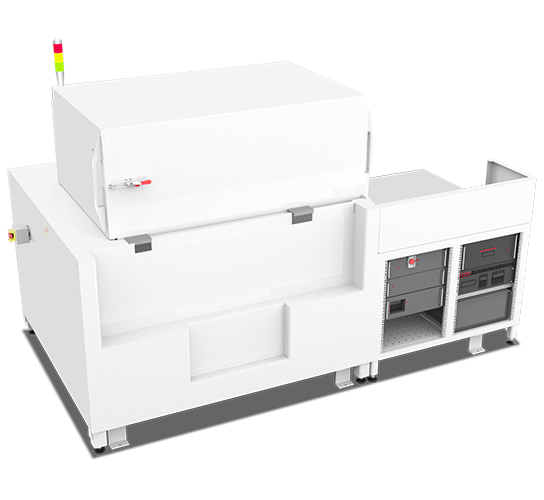
X-ray Assisted Device Alteration (XADA)
First X-ray based Circuit Debugging
Enables New Backside Power Delivery (BPD) Schemes
|
Specifications |
Downloads |
Contact |
|---|
Key Advantages:
- First commercial XADA system
Demonstrated ability to induce time delays in circuits - Microns-scale x-ray probing at high flux density
Achieve down to single digit microns (1-5 µm) - Designed for testers
Designed from the ground up for maximum flexibility in accommodating a wide variety of testers
______________________________
First X-ray Assisted Device Alteration System
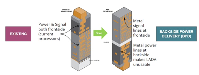
X-ray assisted device alteration (XADA) is the x-ray equivalent of laser assisted device alteration (LADA). In XADA, a highly focused, high-flux-density beam of x-rays induces a perceptible time delay in circuits to rapidly isolate critical signal paths (“speedpaths”). Sigray’s XADA-200 is a critically needed solution for circuit debugging in for emerging backside power delivery (BPD) schemes, where power lines are moved to the backside of the device (see image below).
BPD is widely considered to be the future of integrated circuit design, enabling improved efficiency and speed for high-performance chips in automobiles, mobile devices, and AI-processing. The challenge is that BPD renders LADA obsolete because devices can no longer simply be thinned on the backside to allow a NIR laser to penetrate and induce a photoelectric current (or locally heat the area). Due to the penetrating power of X-rays, XADA not only enables circuit debugging in new BPD devices but also requires little to no sample preparation (e.g., backside thinning).
_______________________
Microns-Scale X-ray Probing
XADA’s small probe size is enabled by patented and patent-pending innovations in x-ray source and x-ray optics technologies.
Sigray is the world leader in x-ray optics and has developed advanced fabrication capabilities under several large government grants over the past decade. The company now supplies its x-ray focusing optics to most synchrotron facilities. Due to its heavy R&D investment in x-ray optics, Sigray is the only company in the world capable of fabricating double-paraboloidal x-ray optics with the stringent straightness and surface profile tolerance requirements needed for XADA. Optics used for XADA are produced through a patent-pending process that maximizes symmetry and minimizes slope errors. Additional patent-pending innovations in x-ray source and optics are expected to enable Sigray XADA probes to achieve submicron spot sizes in the future
Using X-rays, 3-4 ps shifts in circuit delays can be seen
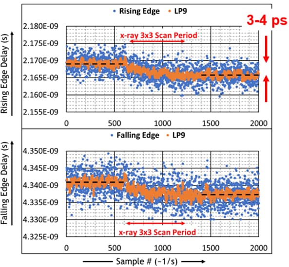
3-4 delay ps delay seen using Sigray XADA
______________________________
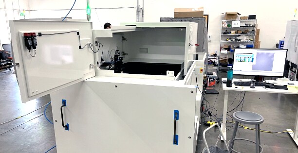
Configured and Designed for Testers
Sigray collaborated with industrial thought leaders to develop a system with a large, flexible tester area to accommodate a wide variety of tester designs. To reduce costs associated with expensive tester cables, the system was also designed with large cable runs, minimizing cable lengths and allowing testers to be moved into and out of the XADA unit without disconnecting the cables.
Technical Specifications of XADA
|
|
Parameter |
Specification |
|---|---|---|
|
Overall |
Probe Size |
<5 μm standard. 1-3 μm available as upgrades. |
|
Operating Energies |
Selectable between 5-9 keV |
|
|
Time Shift |
Shift is linear to x-ray exposure. Examples include a 3-4 ps timeshift noted (will be reported at IPFA). |
|
|
Source |
Type |
Sigray patented ultrahigh brightness sealed microfocus source |
|
Target(s) |
Standard 3 target x-ray source. Selectable from Si, Cr, Cu, Rh, W, Mo, Au, Ti, Ag. Others available upon request. |
|
|
Maximum Power | Voltage |
30W | 45 kVp |
|
|
X-ray Optic |
Type |
Sigray patent-pending x-ray optics |
|
Dimensions |
Footprint |
WLH: 1.7 x 2.9 x 2 meters |
|
Stage Travel |
150 x 150 mm automated travel |
|
|
Additional Capabilities |
Other Modalities |
Visible light and/or IR navigation available |
|
Software |
Custom CAD navigation |
*Note: For academic institutions with smaller budgets, Sigray offers a XADA “Lite” version with reduced specifications and flexibility. Inquire with your local sales representatives or fill out the Contact Us form at the bottom of this page.