Products & Technologies

Products & Services
Company
Contact
Products & Services
Products & Technologies
Services
Resources
Company
Contact
Accelerating AI innovation at the EPIC Center
From breakthroughs to ramp-ready solutions, faster than ever
Industry’s best innovators and most advanced tools
Innovating together, multiple generations into the future
R&D without handoffs
Compressing the path from concept to commercialized chip
In the race for AI compute leadership, the EPIC Center accelerates innovation and commercialization of new chip technologies—from creating breakthroughs to ramp-ready solutions—faster than ever before.
-
~$5B
Capital investment — Applied's largest ever
-
600,000ft2
Purpose-built for commercialization
-
4 acres
Advanced cleanroom space
See what’s happening now across EPIC
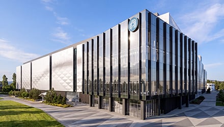
Applied Materials Unveils $5 Billion EPIC Center in Silicon Valley to Accelerate Semiconductor Innovation for the AI Era
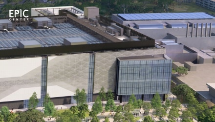
Applied Materials and UCLA Engineering Accelerate Semiconductor Innovation at the EPIC Center
Applied Materials and Intel Collaborate to Accelerate Chipmaking Innovations for AI-Driven Computing

EPIC sets the pace for AI acceleration
Co-Innovation
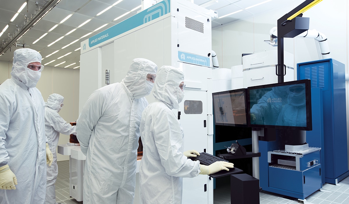
Chipmakers, designers, researchers and Applied’s scientists side-by-side, compressing the path from concept to commercialized chip.

High-Velocity
Innovating the way we innovate to work securely in parallel and accelerate how fast an invention becomes a qualified process running at volume.
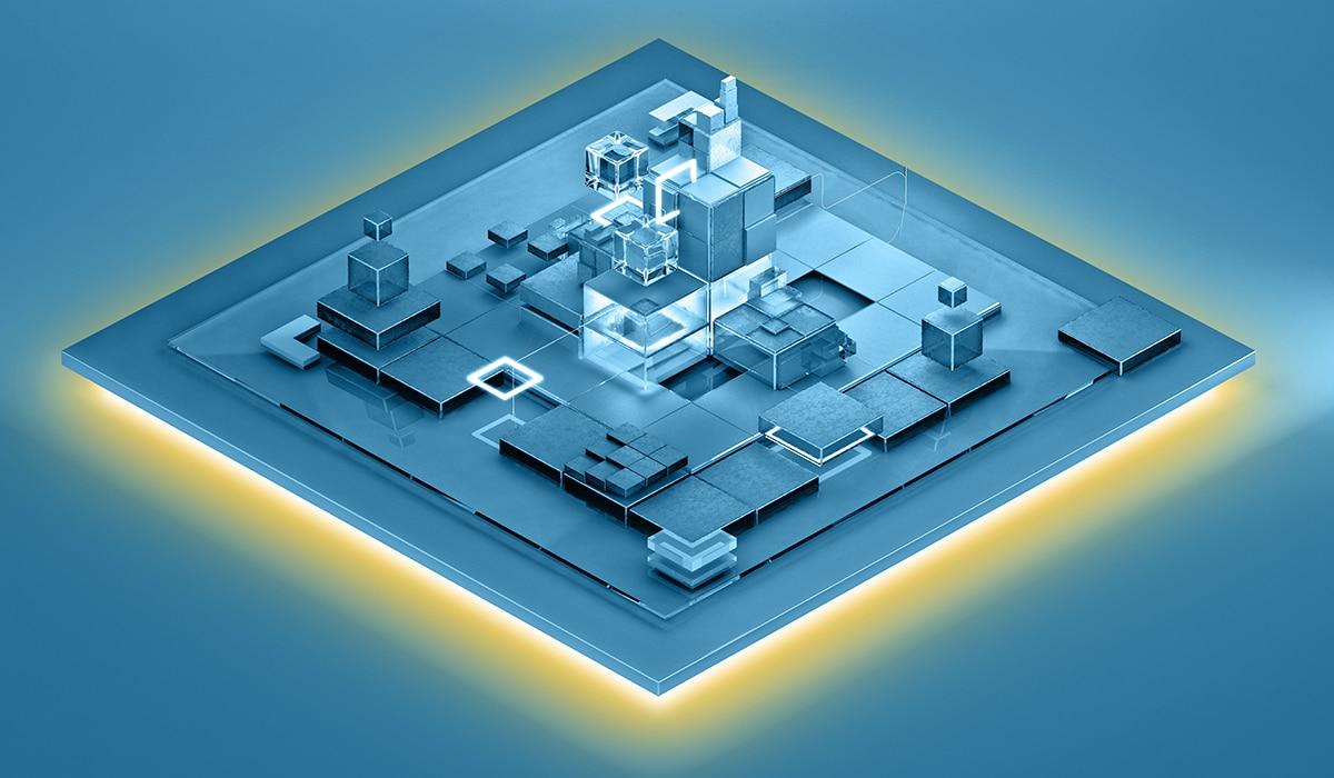
Commercialization
Processes leave EPIC ready to ramp, accelerating the path from breakthrough research to pilot lines, & getting to high yields faster in high-volume manufacturing.
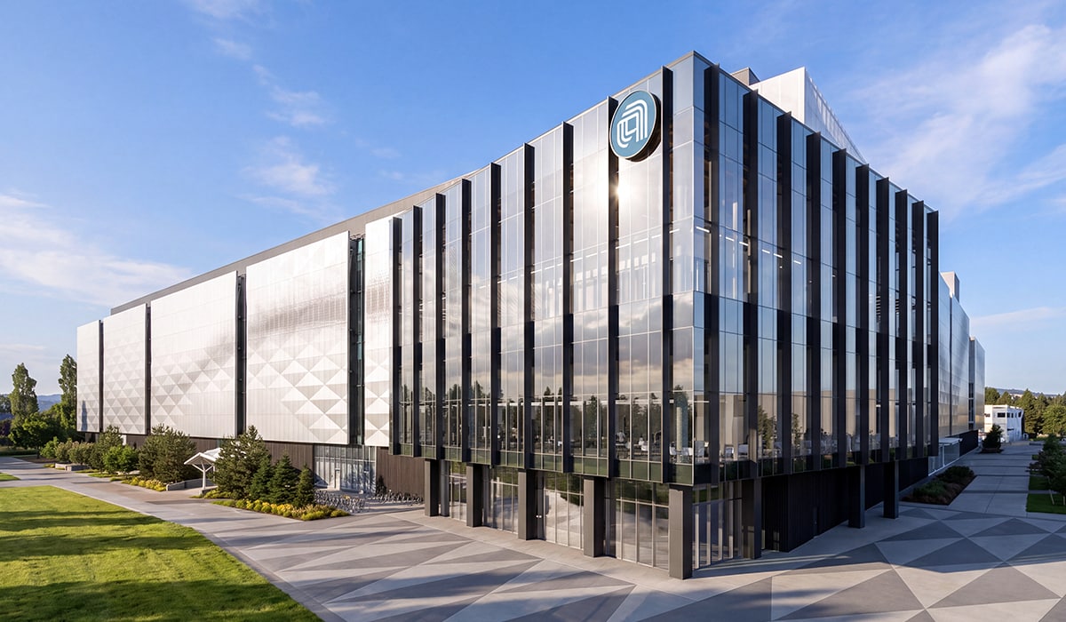
Smarter R&D
Working several generations ahead with earliest access to next-generation materials and equipment means secure, smarter R&D bets and design that ramps faster.

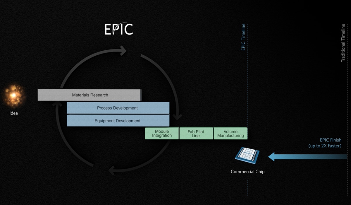
A new R&D model to drive chip technology forward, faster
In the race for AI compute leadership, the EPIC Center accelerates innovation and commercialization of new chip technologies—from creating breakthroughs to ramp-ready solutions—faster than ever before.
At EPIC, the world’s leading chipmakers will work alongside our scientists and engineers to compress the time from concept to commercialization, delivering the best chip and packaging architectures with the fastest time-to-yield. That is how we deliver material innovation that changes the world – faster.
Gary Dickerson President and CEO Applied Materials

Explore the EPIC Center
Frequently Asked Questions
Applied Materials’ Equipment and Process Innovation and Commercialization (EPIC) Center is a collaborative innovation facility in Silicon Valley, built to accelerate how new chip technologies move from early research to high-volume manufacturing. Inside EPIC, chipmakers, systems companies, equipment partners and university researchers work alongside Applied’s scientists and engineers on technology three to four generations ahead of production. By developing in parallel rather than in sequence, EPIC shortens learning cycles, delivers more mature technology to customers’ factories, and makes every R&D dollar go further—material innovation that changes the world, made faster.
The EPIC Center is on Applied Materials’ campus in Sunnyvale, California, in the heart of Silicon Valley, chosen for its proximity to the world’s leading chipmakers, systems companies and universities.
Semiconductor R&D has traditionally run as a relay: research in one place, equipment and process development in another, integration and pilot production in a third, with a handoff at every stage. Those handoffs have cost the industry years at a time, and the AI era does not have years to give. EPIC exists to remove them.
For chipmakers, the EPIC Center will provide earlier access to Applied’s R&D portfolio, faster cycles of learning and accelerated transfer of next-generation technologies into high-volume manufacturing, within a secure collaborative environment.
For university researchers, the EPIC Center offers a rare opportunity to pursue manufacturing-relevant research in an industry-scale environment, enabling rapid iteration, faster validation, and smoother transition from discovery to deployment. Working alongside Applied scientists and engineers, academic teams gain access to cutting-edge equipment and process integration that can shave years off the traditional new materials development cycle.
Yes — as part of a decarbonization strategy, the building is equipped with an all-electric central volatile organic compound (VOC) abatement unit, and the central facilities equipment has been electrified, eliminating stationary combustion Scope 1 emissions associated with central boilers.
The EPIC Center is also designed to recycle/reuse approximately 40% of its water.
EXPLORE MORE
Discover how Applied Materials connects people, ideas and opportunities to enable breakthroughs that deliver material innovation.