Products & Technologies
Products & Services
Company
Contact
Products & Services
Products & Technologies
Services
Resources
Company
Contact
Applied Materials Germany
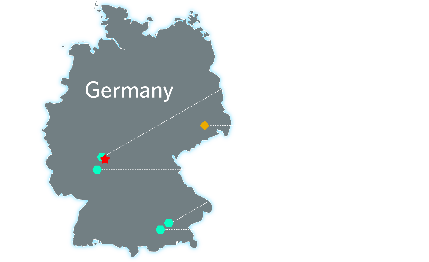

Leading European Semiconductor Operations
Germany hosts Applied Materials' largest European operations, with facilities strategically located in Bavaria, Hesse, and Saxony. Our presence in these key regions allows us to serve customers across Germany and neighboring areas with unparalleled expertise and cutting-edge technology. Germany’s manufacturing strength and engineering culture make it a cornerstone of Applied Materials’ European operations.
We Are Applied Materials Germany
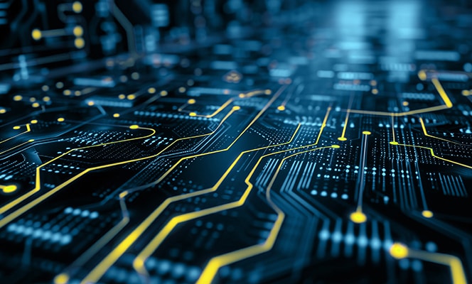
Our cutting-edge innovations, such as ultra-clean magnetic levitation transport systems and high-resolution electron beam columns, enable us to design advanced systems and solutions that power the intelligence behind every electronic device.
Our Focus
Customer and Product Support
Our Dresden facility is a hub for sales support, system installation, maintenance, software, and other services for semiconductor production equipment. Conveniently located near customers in Central Europe, including some of the world's leading semiconductor device manufacturers, we provide state-of-the-art technological resources to anticipate and meet the needs of our customers. We help them build semiconductor chips that power IoT, communication, automotive, power, and sensor applications.
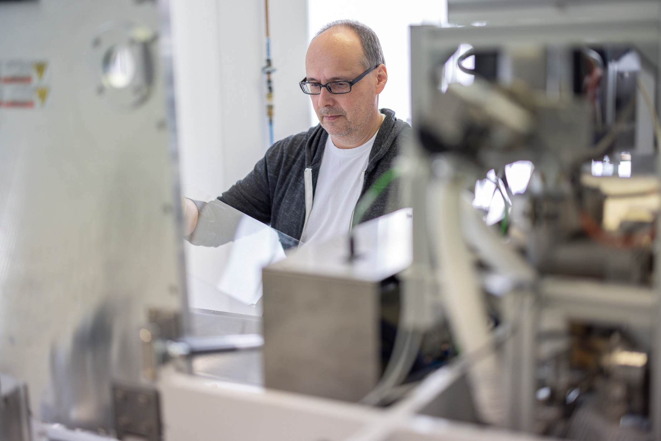
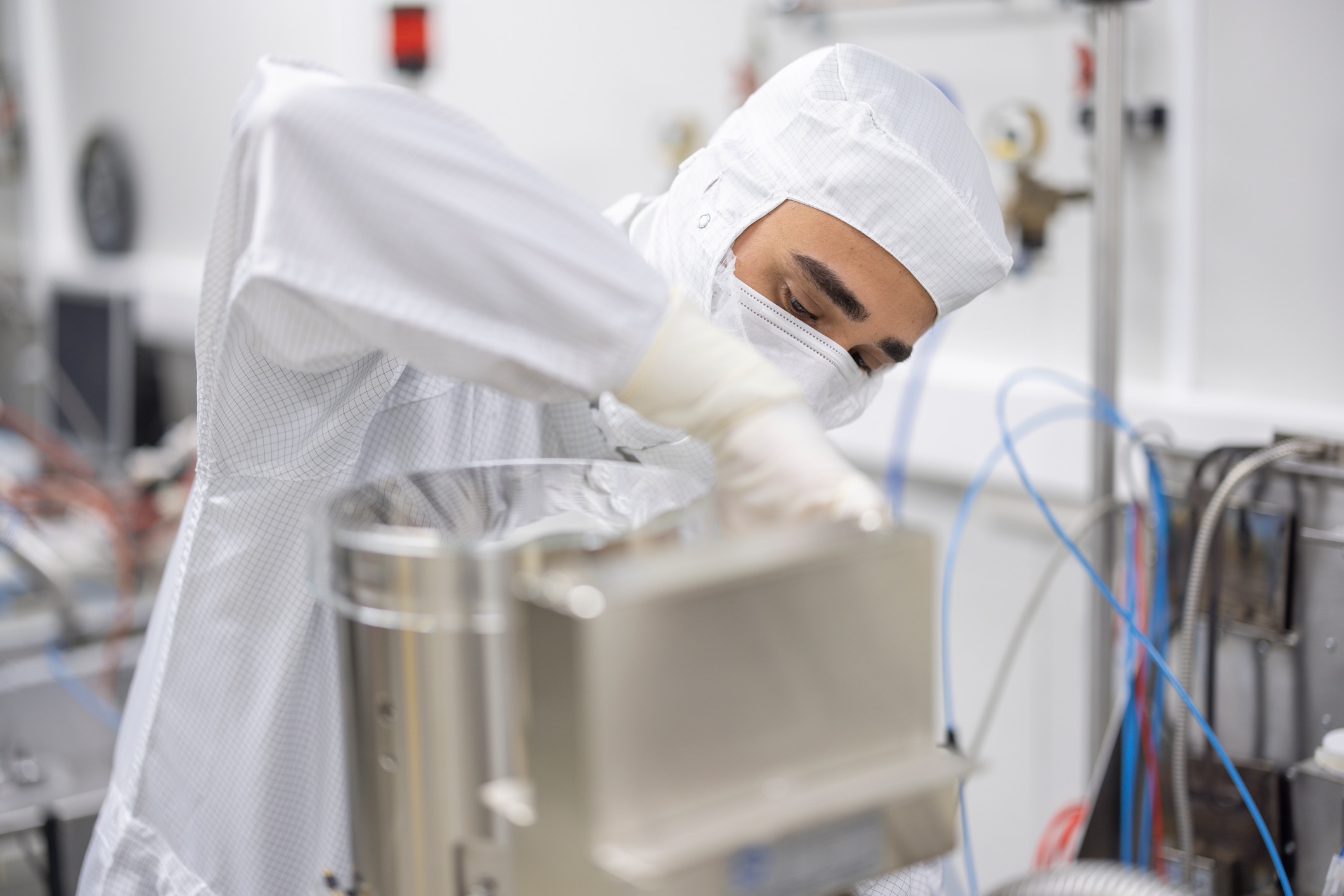
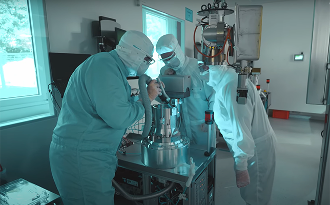
Manufacturing and R&D
In Alzenau, we specialize in developing advanced display and OLED technologies, offering solutions for a broad range of applications, from architectural designs to packaging solutions.
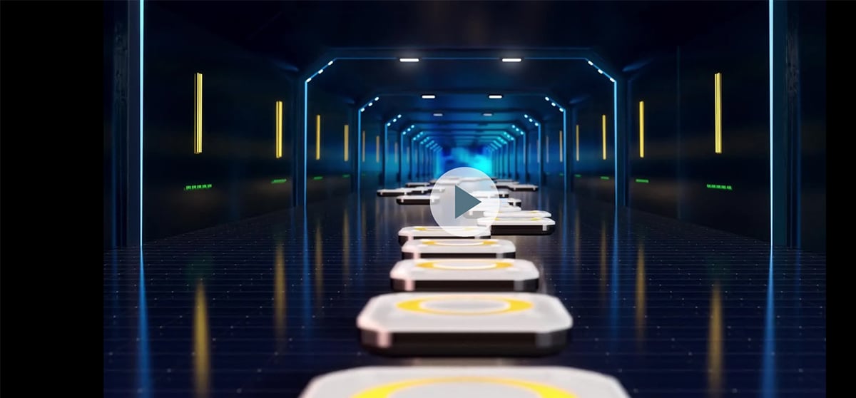
In Darmstadt, we innovate contactless motion systems using magnetic bearings to enhance our manufacturing processes. These levitation systems are crucial for display and semiconductor applications, ensuring ultra-clean and ultra-high vacuum environments where conventional transportation methods would compromise production yield. Our systems produce end-user products ranging from memory chips to CPUs and displays for smartwatches, VR goggles, monitors, and TVs.
In Darmstadt, we innovate contactless motion systems using magnetic bearings to enhance our manufacturing processes. These levitation systems are crucial for display and semiconductor applications, ensuring ultra-clean and ultra-high vacuum environments where conventional transportation methods would compromise production yield. Our systems produce end-user products ranging from memory chips to CPUs and displays for smartwatches, VR goggles, monitors, and TVs.
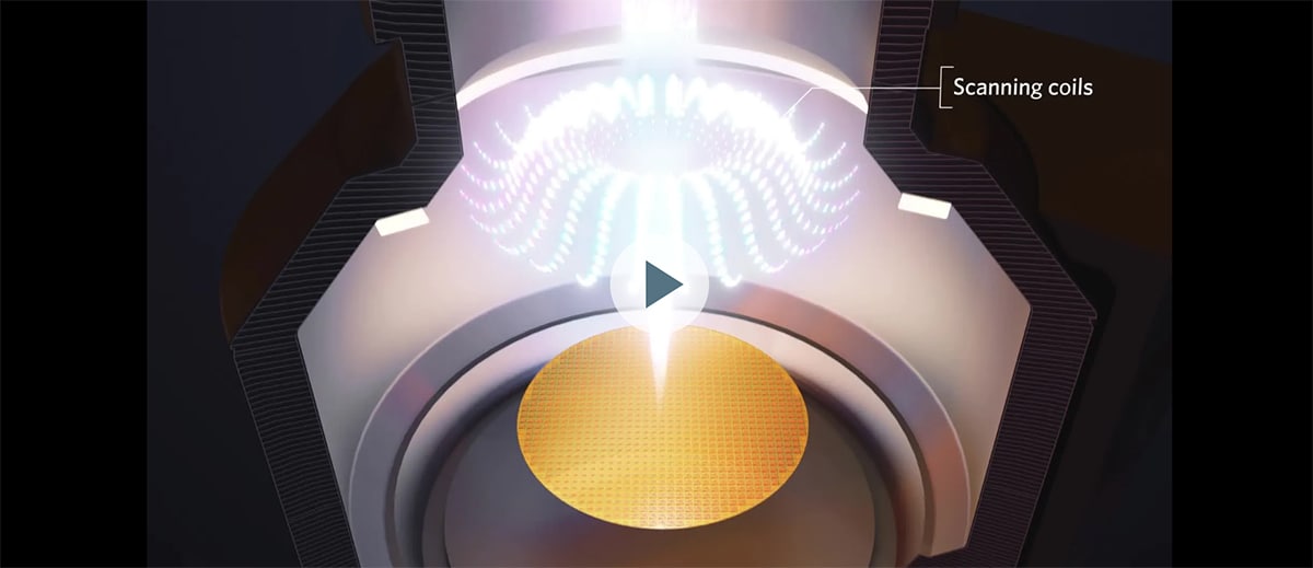
In Munich, we collaborate closely with our global network of experts to research, develop, and manufacture high vacuum electron beam columns at our Feldkirchen and Heimstetten locations. These solutions are integrated into advanced semiconductor production equipment at our metrology and inspection operations in Israel and our display and test equipment manufacturing sites in Taiwan. Our technology can detect particles as small as 1nm on a 300mm silicon wafer, equivalent to finding a single grain of sand in a football stadium.
In the News
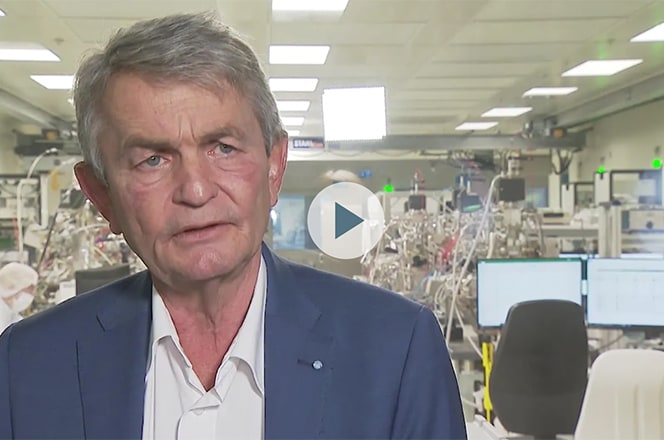
Euronews
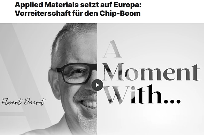
News article featuring Florent Ducrot, Applied Materials Head of European Operation: Read Article
Die Welt
Featured article about Applied Materials presence in Germany: Read Article
TBD Media
Featured video about Applied Materials presence in Germany: Watch Video
Mehr als Ein Probetag
An der Zukunft Schrauben mi Applied Materials: Watch Video
SAT1 Bayern
Regional TV interview and featured video about Applied Materials presence in Bavaria