Products & Technologies
Products & Services
Contact
Products & Services
Products & Technologies
Services
Resources
Contact
Posted
July 05, 2023

Stay updated on our content.
Semiconductor Equipment and Processes Need Digital Twins

by Umesh Kelkar
July 5, 2023
Since they were first described in 2002[1], there has been remarkable interest in developing and deploying digital twins to enable and accelerate smart manufacturing across many industries. While we have seen growing excitement in the technology within the semiconductor equipment industry, we are still in the very early innings of creating and capturing value from digital twins.
Applied Materials plays an enabling role in driving the advances in computing power needed to accurately model and simulate the physical world. Today, we are taking advantage of this same technology to help address the growing complexity of chip process technology, which is driving up R&D costs and increasing the time it takes to bring new technologies to high-volume production.
Digital Twins Can Help
We must use every tool in our toolbox to help manage this increasing cost and complexity. Digital twins give us opportunities to advance the roadmap in novel ways, accelerating concept creation, process exploration, prototyping, testing, knowledge sharing and talent development. Recent trends in the integration of sensors and metrology, along with advances in modeling and algorithms including artificial intelligence, bring us to the point where we can overcome the cost and complexity challenges.
As previewed in our 2021 blog, “Taking a Second Look at ‘AI’,” a digital strategy has many applications across the process node lifecycle, from R&D to process transfer, ramp and high-volume manufacturing. Examples include system and chamber matching, performance and productivity improvement, diagnostics, predictive maintenance and accelerating “green to green” times between tool maintenance and recovery.
At Applied, our vision is a holistic digital twin architecture representing the entire semiconductor process flow. We are developing digital twins of materials, process equipment, metrology, on-chip structures and electrical performance. In addition, with the growing focus on sustainable semiconductor industry growth, our digital twin strategy includes modeling the carbon emissions of alternative semiconductor materials, recipes and manufacturing techniques.
AppliedTwin™ Framework: A Practical Digital Twin Solution for Semiconductor Manufacturing
The AppliedTwin™ framework is the name of our digital twin solution for semiconductor manufacturing equipment and processes. We are developing a flexible platform that models the complexities of manufacturing from micro to macro: from the smallest on-wafer features to the performance of an entire fleet.
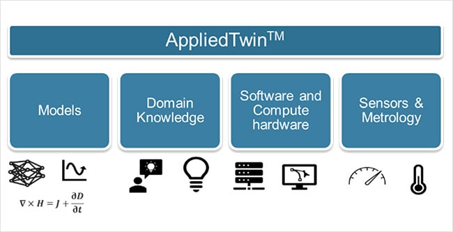
The AppliedTwin framework virtualizes processes and equipment using the best available models, informed by sensor and metrology data, guided by domain knowledge, and continuously synchronized with their physical counterparts. The framework is designed to predict equipment performance and process outcomes with fidelity to provide actionable insights to the user.
Inviting Collaboration
The promise of digital twins equals the weight of the challenges we face in driving the semiconductor roadmap forward with speed and R&D efficiency. Collaboration will be key. Applied recently announced plans to open the Equipment and Process Innovation and Commercialization (EPIC) Center, and we are already planning to make digital strategies a key pillar of the collaborative work with our customers along with university and industry partners. The EPIC center will be a place to test the interoperability and efficacy of digital twins for the semiconductor manufacturing ecosystem.
As the industry’s broadest supplier of wafer fab equipment, Applied is well positioned to help drive the adoption of digital twins and accelerate the roadmap. Stay tuned for more news about how we are advancing our AppliedTwin framework.
[1] Grieves, Michael. (2002). SME Management Forum Completing the Cycle: Using PLM Information in the Sales and Service Functions.
Umesh Kelkar, Ph.D.
Managing Director, Computational Products and Solutions

Dr. Umesh Kelkar leads the Computational Products and Solutions team which enables Applied Materials’ product development through multi-physics and multi-scale computational modeling and simulation. He is also responsible for Applied’s commercial multi-physics software suite ACE+. In addition, he leads vision, strategy and execution for the AppliedTwin™ framework.
Umesh joined Applied in 1997 as a process engineer after receiving a master’s degree and Ph.D. in mechanical engineering from the University of Arkansas, Fayetteville.
A New Equipment Platform for a New Era of Chipmaking
Most semiconductor industry observers know it takes hundreds of process steps to make a chip. They can picture overhead transfer systems speeding orange FOUPs (Front Opening Universal Pods) full of wafers from tool to tool, imagining each process step being executed as quickly as physics allows before the wafers are zipped off to the next machine. They can sense the science behind the high-stakes race to produce the most precisely completed wafers in the shortest possible time.

Doubling Down on Collaboration at SEMICON West 2023
The semiconductor industry has proven itself more than capable of achieving growth by collaborating to overcome big challenges. Collectively, we have demonstrated innovation and resiliency that is fueling what several industry analyst firms project will be a $1 trillion semiconductor market by 2030 that could directly seed $3-4 trillion of global electronics growth.

Taking a Second Look at “AI”
Applied Materials technology has long been used by our customers to build the chips that AI runs on. Our ExtractAI™ technology provides a real-time, intelligent link between our Enlight® optical wafer inspection system and our industry-leading eBeam review system, SEMVision®, allowing the power of adaptive AI-based pattern recognition to be used to give process engineers “Actionable Insights” about yield-killing defects.