Products & Technologies
Products & Services
Contact
Products & Services
Products & Technologies
Services
Resources
Contact
Posted
July 11, 2023

Stay updated on our content.
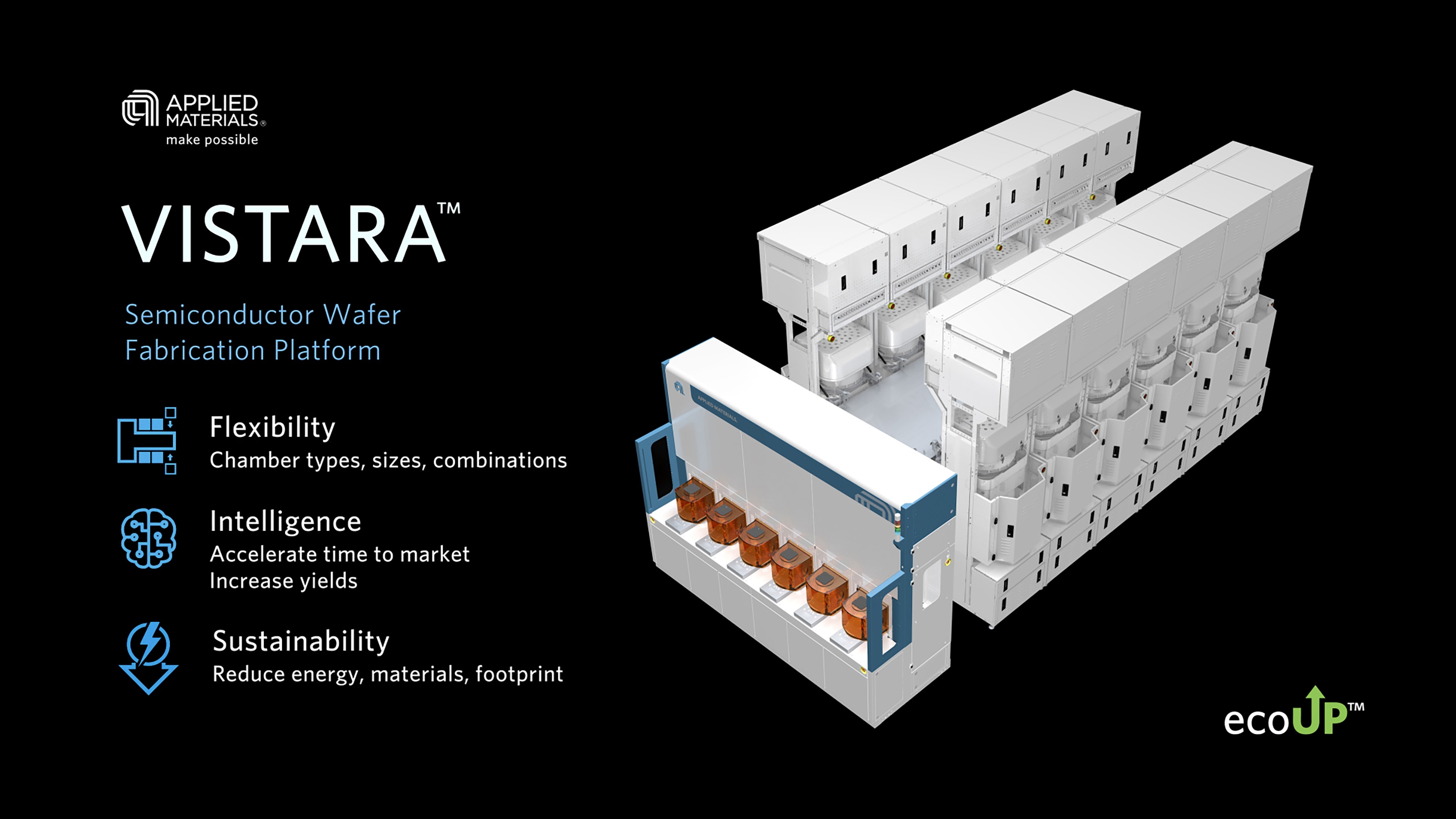
A Deeper Look into the New Vistara™ Platform
by Applied Blog
July 11, 2023
Today marks a major milestone in Applied Materials history. At SEMICON West 2023, we introduced Vistara™, a wafer manufacturing platform designed to provide chipmakers with the flexibility, intelligence and sustainability needed to tackle growing chipmaking challenges.
This is not your run-of-the-mill equipment launch. Vistara is Applied’s most significant new platform in more than a decade – a purpose-built system that has been expertly designed over the past four years by hundreds of engineers from across Applied’s hardware, software, process technology and ecoefficiency teams.
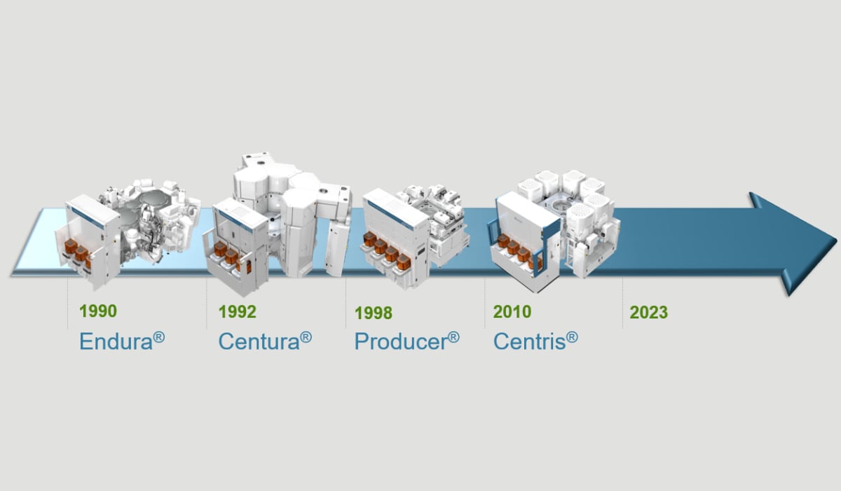
When we introduce a new platform, it is designed to be a be a trusted solution for many years of customer innovation, reliability and productivity. We ship thousands of new systems to customers each year, and most have been based on just four major platforms that were introduced and refined over the past three decades. To learn more about the history and longevity of Applied’s equipment platforms, read this blog from Applied Fellow Mike Rice.
The new Vistara platform is architected based on three pillars: flexibility, intelligence and sustainability. The following animation video highlights the capabilities and components behind each of these pillars:
The Vistara platform was launched this morning during Applied’s SEMICON West Technology Breakfast event. More information about the event, including presentations, press releases and other materials, can be found on the Investor Relations Events page of our website.
Applied Materials
Corporate Communications
The Applied Materials team publishes posts of general interest to our readers.

Semiconductor Equipment and Processes Need Digital Twins
Since they were first described in 2002, there has been remarkable interest in developing and deploying digital twins to enable and accelerate smart manufacturing across many industries. While we have seen growing excitement in the technology within the semiconductor equipment industry, we are still in the very early innings of creating and capturing value from digital twins.
A New Equipment Platform for a New Era of Chipmaking
Most semiconductor industry observers know it takes hundreds of process steps to make a chip. They can picture overhead transfer systems speeding orange FOUPs (Front Opening Universal Pods) full of wafers from tool to tool, imagining each process step being executed as quickly as physics allows before the wafers are zipped off to the next machine. They can sense the science behind the high-stakes race to produce the most precisely completed wafers in the shortest possible time.

Doubling Down on Collaboration at SEMICON West 2023
The semiconductor industry has proven itself more than capable of achieving growth by collaborating to overcome big challenges. Collectively, we have demonstrated innovation and resiliency that is fueling what several industry analyst firms project will be a $1 trillion semiconductor market by 2030 that could directly seed $3-4 trillion of global electronics growth.