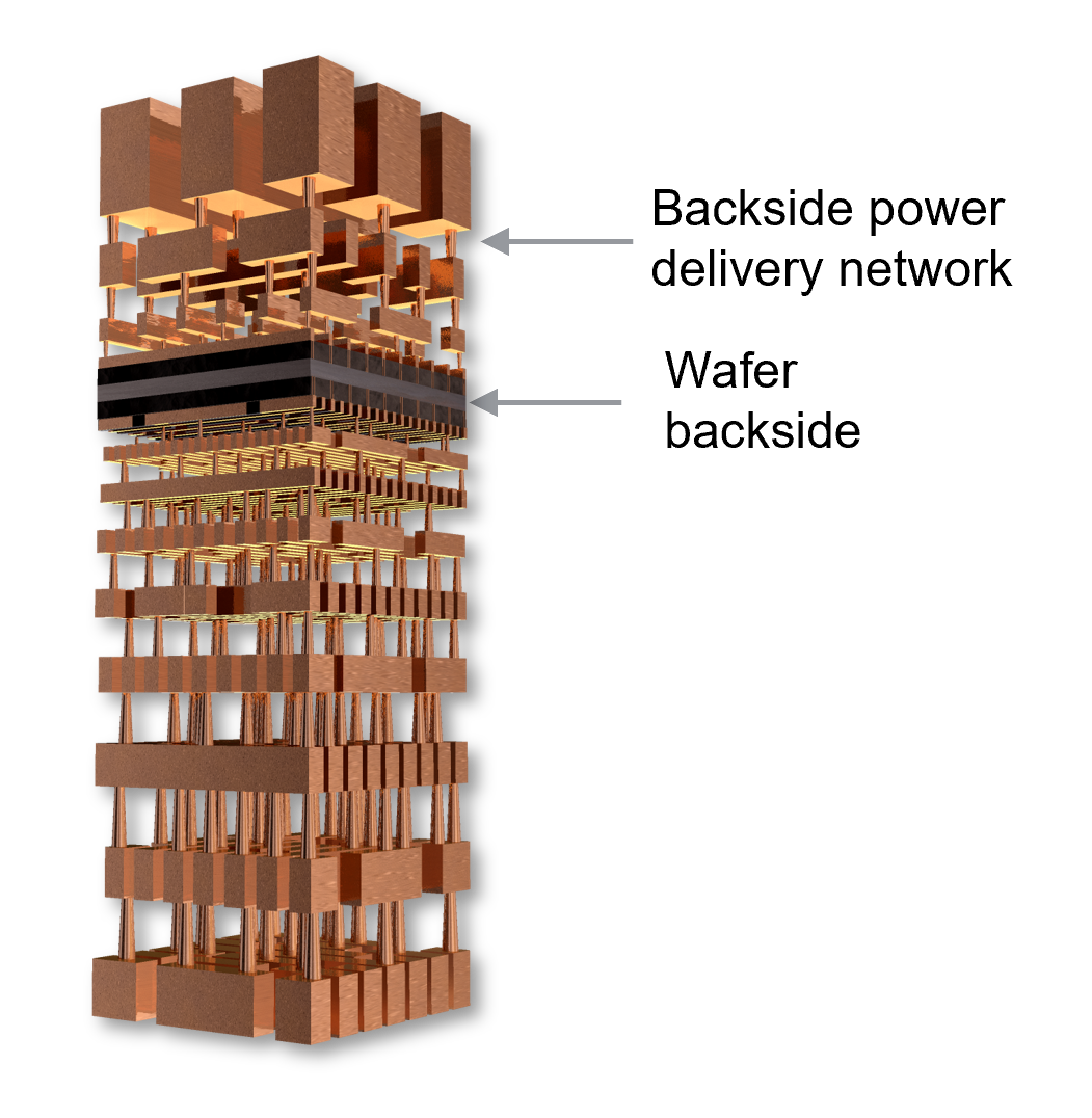
Backside Power Delivery
All silicon chips today have power delivered from the frontside of the chip. This requires power to be delivered through over 10 layers of wiring, down to the transistor. There are two major limitations of this approach: valuable real estate on the chip must be allocated for power lines, and power is lost as it traverses the multiple levels down to the transistor.
Backside power delivery refers to the technique of routing power supply lines on the backside of a semiconductor chip or integrated circuit (IC) instead of the traditional frontside. This approach increases logic density and improves power and performance.
Innovative device architectures, new materials development, monolithic and heterogeneous integration of materials, larger wafer sizes, and single-wafer processing are required for these technologies to meet today’s application requirements. The ongoing development and evolution of 200/300mm production technologies deliver device and yield improvements as well as overall fab productivity gains - all of which translate into sustained performance and cost benefits for semiconductor manufacturers.
Backside power delivery will use many of the technologies used in transistor contact and interconnect engineering. Our leadership position in interconnect and front-end technologies puts Applied Materials in a unique position to enable and accelerate the adoption of this technology. Our portfolio of products includes chemical mechanical planarization (CMP), dielectrics deposition, etch, epitaxy, implant, anneals, atomic layer deposition (ALD), and metals deposition as well as our IMS® capabilities, which will be key to achieving the breakthroughs needed to enable backside power delivery.
More information on Backside power delivery can be found on our Master Class and blogs on this topic.