Advanced Logic
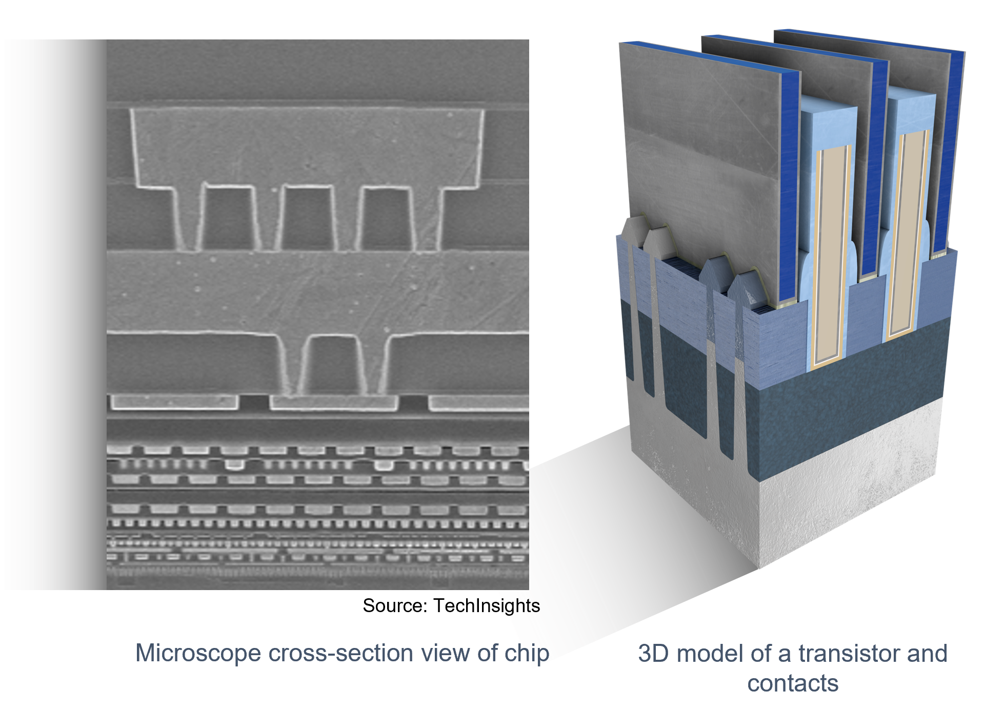
Advanced logic chips are found in almost every device we use, from smartphones to tablets to smartwatches. Did you know the heart of the smartphone is the CPU or central processing unit? It determines the user experience–and performance and battery life are paramount. Chipmakers are pushing the boundaries of advanced transistor design and process technology to improve the user experience. Today’s state-of-the-art smartphone processor, built with the most advanced logic technology, incorporates over 16 billion transistors and 32 billion transistor contacts.
This advanced logic technology is the culmination of many semiconductor process innovations that have occurred over several decades. We are now in the advanced FinFET era, and the industry is transitioning to a new transistor architecture called Gate-All-Around (GAA).
At Applied, we enable these innovations with our leadership in materials engineering. Key technologies that enable the transistor roadmap include epitaxy, ion implant, rapid thermal processing, chemical mechanical planarization (CMP), and a special kind of etch called selective materials removal. We combine these technologies in unique ways to enable integrated materials solutions (IMS®), where multiple process steps take place in one system for the best possible performance and power results.
To enable further logic scaling requires innovations in transistor and interconnect design as well as patterning and DTCO or Design Technology Co-optimization. This section covers FinFET and gate-all-around transistors, as well as interconnect technologies and an innovation called backside power delivery.
More information on these topics can be found on our Master Class and blogs.