Products & Technologies

Products & Services
Company
Contact
Back to Menu
Products & Services
Products & Technologies
Services
Resources
Company
Contact
Posted
June 10, 2021

Stay updated on our content.
New Innovations Needed to Continue Scaling Advanced Logic
Jun 10, 2021
The semiconductor industry is at a crossroads. Demand for chips has never been greater as we enter the early stages of a new wave of growth fueled by the Internet of Things, Big Data and AI. At the same time, it’s become apparent that conventional Moore’s Law 2D scaling techniques are no longer able to deliver the consistent improvements in power, performance, area-cost and time to market (PPACt) that chipmakers have long relied on. This is particularly the case for logic chips, which serve as the main processing engine in nearly every electronic product and where power efficiency and performance are critical.
To shed light on this issue, Applied Materials is hosting an online Logic Master Class on Wednesday, June 16. I will be joined by other experts from Applied and the industry to discuss the logic scaling roadmap, including challenges and solutions for delivering continued improvements in PPACt. We will be exploring several different areas, including transistor and interconnect scaling, patterning and design technology co-optimization (DTCO). The common denominator underlying all of these areas is the need to supplement classic 2D scaling with a combination of approaches that includes new chip architectures, new 3D structures, novel materials, new ways to shrink features and new ways to connect chips with advanced packaging.
In this blog, the first in a series, I will give a preview of some of the topics that will be discussed during the Logic Master Class, specifically related to transistor design and the physical limitations that must be overcome to enable advanced logic scaling.
Transistor Switching Speed and Variability
The transistor operates as a switch. To render the best performance, we focus primarily on reducing switching delay by maximizing drive current and reducing capacitance and resistance. In a FinFET transistor, for example, we increase speed by tuning various physical parameters including fin height, the gate length of the channel, the mobility of electrons running across the channel, the threshold voltage used in switching and the thickness of the gate oxide that helps control the switch’s on-off state. We reduce electrical resistance by engineering higher activated dopant atoms in regions adjacent to the channel.
Another critical lever is transistor variability, because performance is gated by the slowest transistors in a given circuit. By tightening the distribution to reduce variability, we can enable faster circuits.
FinFET Performance Barriers Explained: Fin Bending
Let’s zoom in more closely on the most pressing challenges to next-generation FinFET designs. FinFET construction can be divided into three primary modules: channel and shallow trench isolation, high-K metal gate (HKMG) and the transistor source/drain resistance module (see Figure 1).
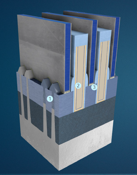
Figure 1: Primary modules of a FinFET are channel and shallow trench isolation (1), high-k metal gate (2) and transistor source/drain resistance (3).
In the channel and shallow trench isolation module, the industry has been increasing fin height and reducing fin width over several technology nodes to increase speed. We are reaching a point, however, where taller, narrower fins are more susceptible to bending during the manufacturing process due to strains caused by the isolation oxide that needs to be placed between the fins. This bending causes counteractive strain which degrades electron mobility and impacts threshold voltages, resulting in increased transistor variability (see Figure 2). To counteract fin bending requires new materials engineering solutions.
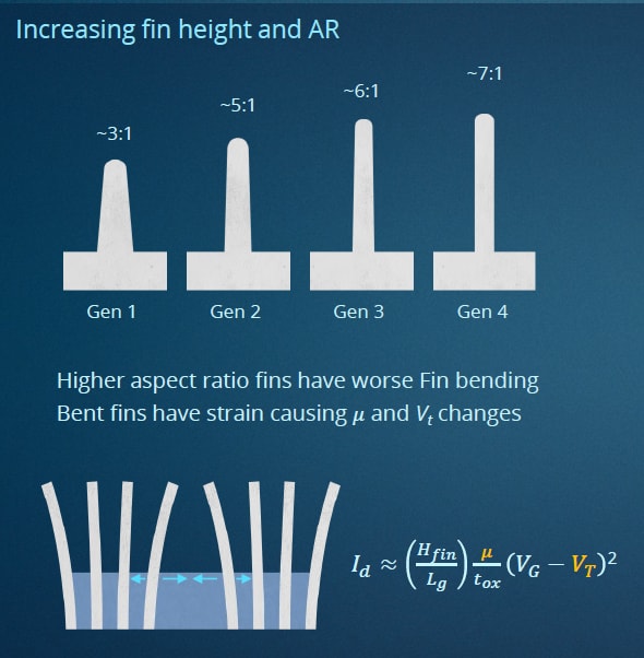
Figure 2: As FinFETs have scaled, the fins that form the gate of the transistor have become taller and narrower, making them more fragile and susceptible to bending during the manufacturing process, which degrades performance and power efficiency.
Restoring Interface and HKMG Scaling Parity
The HKMG module is the heart of the transistor. These metal stacks are highly complex and can contain upwards of seven layers, including the interface, high-k and metal-gate layers (see Figure 3). Interface and high-k scaling are critical to gate-oxide reduction, which boosts transistor drive current. The metal gate is tuned to ensure the transistor has the correct work function, which determines the threshold voltage. The issue is, since the 14nm node, the interface and high-k layers haven’t scaled at the same rate as other physical parameters that make higher transistor drive current possible. New innovations are needed to restore interface and high-k scaling parity.
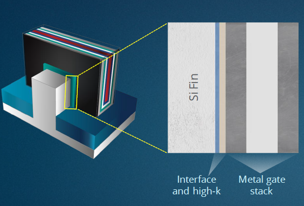
Figure 3: Cross section of a high-k metal gate stack. Scaling the interface and high-k is critical to gate-oxide reduction, which boosts transistor speed.
Contact Volume Eroded with Each New Process Node
The third major transistor element is the transistor source/drain resistance module. Each new process shrink has reduced transistor contact area by roughly 25 percent per node. The smaller area drives up resistance. The main contributors are interfacial resistance between the metal contact and silicon transistor, and external resistance within the source and drain regions (see Figure 4).
Mitigating interfacial resistance and external source/drain resistance requires new materials and the co-optimization of multiple process steps.
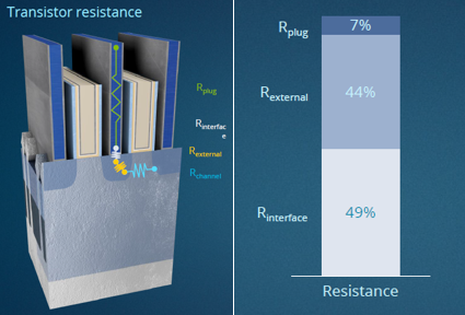
Figure 4: The main contributors to transistor contact resistance are the interfacial resistance between the metal contact and silicon transistor, and external resistance within the source and drain regions.
Laying the Groundwork for Gate-All-Around Transistors
As previously discussed, FinFET fins are becoming unsustainably tall and narrow. Controlling fin width has become harder with each new process shrink, which has led to increased variability in threshold voltages that degrades device performance. The industry is rapidly moving to enable a new architecture called gate-all-around (GAA) where the silicon channels are flipped along their side and stacked up like a layer cake (see Figure 5).
GAA transistors provide a new way to solve channel thickness variability by replacing the traditional lithography- and etch-based control method. Using epitaxy and selective removal instead enables extremely precise thickness control. From a performance perspective, the GAA architecture lowers variability while enabling gate length scaling to increase drive current by 10 to 15 percent, while simultaneously reducing power consumption. Applied Materials is enabling these and other techniques by combining new materials with technologies like selective etch and eBeam metrology, areas we are uniquely positioned to address thanks to the breadth and depth of our technology portfolio.
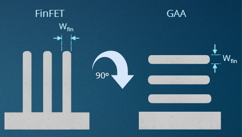
Figure 5: In the gate-all-around transistor architecture, the FinFETs are essentially turned sideways and the channel thickness control changes from lithography and etch to epitaxy and selective removal.
In the next blog in this series, my colleague Mehul Naik, will discuss challenges to reducing resistive-capacitive (RC) delay and power consumption in logic interconnects.
Tags: logic, scaling, PPACt, transistor, interconnect, Patterning, DTCO, 3nm, FinFET, gate all around, high k metal gate, HKMG
Mike Chudzik, Ph.D.
Vice President, Technology

Dr. Chudzik is a Vice President of Technology at Applied Materials. He manages teams of device integrators, process and device engineers and program managers to execute on large scale device fabrication projects. Prior to Applied Materials, Mike was at IBM for 14 years where he led teams in the R&D of advanced semiconductor process integration. He received his Ph.D. in electrical engineering at Northwestern University.

Adding Sustainability to the Definition of Fab Performance
To enable a more sustainable semiconductor industry, new fabs must be designed to maximize output while reducing energy consumption and emissions. In this blog post, I examine Applied Materials’ efforts to drive fab sustainability through the process equipment we develop for chipmakers. It all starts with an evolution in the mindset of how these systems are designed.
Innovations in eBeam Metrology Enable a New Playbook for Patterning Control
The patterning challenges of today’s most advanced logic and memory chips can be solved with a new playbook that takes the industry from optical target-based approximation to actual, on-device measurements; limited statistical sampling to massive, across-wafer sampling; and single-layer patterning control to integrative multi-layer control. Applied’s new PROVision® 3E system is designed to enable this new playbook.
Breakthrough in Metrology Needed for Patterning Advanced Logic and Memory Chips
As the semiconductor industry increasingly moves from simple 2D chip designs to complex 3D designs based on multipatterning and EUV, patterning control has reached an inflection point. The optical overlay tools and techniques the semiconductor industry traditionally used to reduce errors are simply not precise enough for today’s leading-edge logic and memory chips.