
Back to Menu
Endura® Clover® MRAM PVD

The Applied Endura Clover MRAM PVD 시스템은 MRAM 메모리 소자의 대량 생산에 적합한 최초의 통합 소재 솔루션(IMS™)입니다. 플래시 메모리는 전하 기반 작동에 의한 미세화의 한계에 직면하고 있습니다. MRAM은 메모리 반도체의 주요 특징인 비휘발성, 랜덤 액세스 및 강한 내구성을 가지는 동시에 저항 기반 작동으로 미세화를 가능하게 해 플래시 메모리의 대체품으로 가장 유망한 제품입니다.
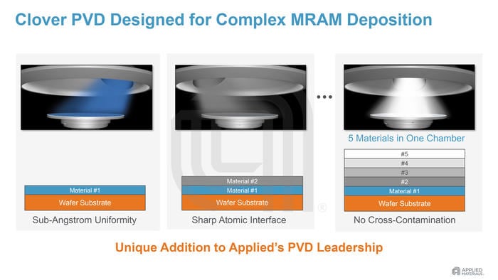
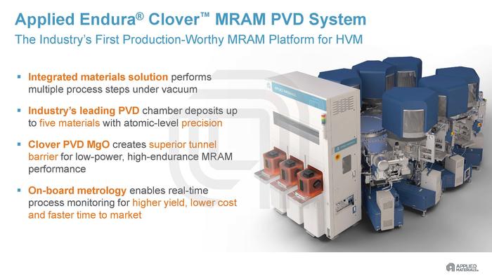
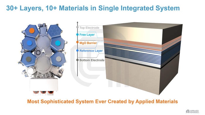
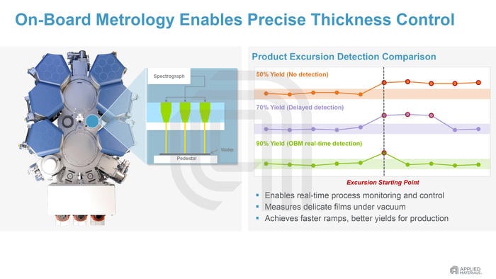
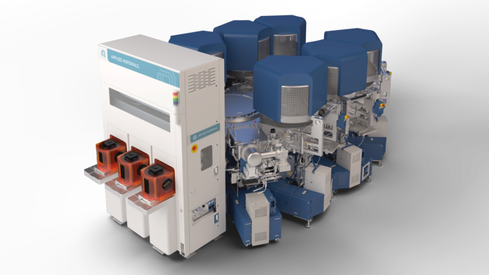
Comprising up to seven deposition chambers configured with pre-clean, anneal, and cooling chambers as well as on-board metrology, the Clover system accommodates production of the entire MRAM stack, which can consist of more than 30 layers—most of which are just a few Angstroms thick—without a break in vacuum. The vacuum environment preserves the quality of the films (which inevitably degrade to some degree if removed from a system during processing), creating high-quality interfaces between layers, reducing the risk of defects, and enhancing the accuracy of the metrology that verifies deposition thickness precision and uniformity—essential for ultimate device performance.
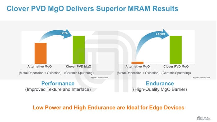
The heart of the Endura Clover system is a chamber capable of depositing up to five different materials with outstanding uniformity. Several of these materials have not previously been used in CMOS technology. To ensure that each film is pristine, a rotating shield above the wafer exposes only one target material at a time to plasma bombardment. This creates optimal interfaces between the layers, essential for device reliability. The performance-critical tunnel barrier layer of magnesium oxide (MgO) is deposited in a separate chamber equipped with specialized hardware that permits one-step deposition of the compound. This improves film integrity and uniformity, minimizes defectivity, and improves the memory read signal by increasing tunnel magnetoresistance (TMR). Subsequent annealing and cryogenic cooling further strengthen the film, fortify the TMR, lower the resistance to facilitate low power consumption, and create high thermal stability for better data retention.
As thickness precision and uniformity requirements are extremely rigorous for the complex MRAM stacks, the Endura Clover system includes on-board metrology to measure and monitor the thickness of critical layers as the stack is created. These measurements are extremely accurate (to 0.2 Angstrom) as the film properties from which the thicknesses are derived have not been altered or degraded by removing the wafer from vacuum. Real-time, layer-by-layer monitoring allows rapid detection of process excursions, which helps improve yields, lower cost, and accelerate time to market—key considerations for HVM.
- 1 / 7
- 2 / 7
- 3 / 7
- 4 / 7
- 5 / 7
- 6 / 7
- 7 / 7