Products & Technologies
Products & Services
Company
Contact
Back to Menu
Products & Services
Products & Technologies
Services
Resources
Company
Contact
Applied PECVD 5.7

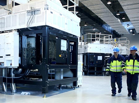
The Applied PECVD 5.7 system deposits the active layers of thin film silicon solar panels on glass substrates up to 5.7m2 in area – the largest in the world. The PECVD 5.7 system is based on Applied’s industry- leading AKT systems for TFT-LCD display manufacturing, proven in over 800 installations worldwide.
The Applied PECVD 5.7 is a single substrate processing system with 7 independent chambers clustered around a central transfer module. It features dedicated amorphous and microcrystalline deposition chambers to eliminate the risk of cross-contamination between the absorber layers of multijunction cell technologies.
- High deposition rate (>500Å/minute for microcrystalline films) enables increased productivity.
- Improved uniformity to enhance cell conversion efficiency.
- Production-proven platform with high uptime (>90%) and superior reliability.
