Products & Technologies
Products & Services
Contact
Products & Services
Products & Technologies
Services
Resources
Contact

Stay updated on our content.
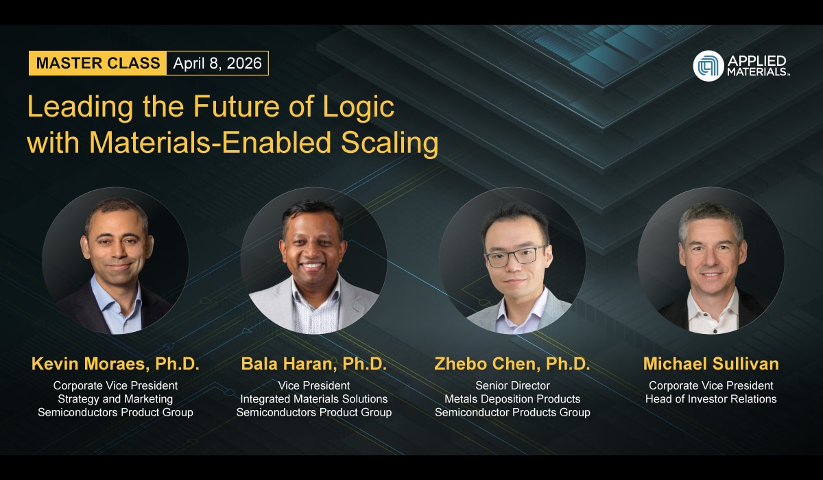
The Angstrom Era Explained: New Master Class Series Kicks Off April 8
March 30, 2026
The semiconductor industry is racing toward $1 trillion in annual revenue, driven by explosive AI demand that has pulled forward years of expected growth into the present. Energy-efficient compute is the defining constraint, but the traditional scaling approaches that have driven the industry are hitting physical limits. At angstrom-scale nodes – where the interplay of individual atoms determines chip performance – materials engineering has become the decisive competitive advantage.
Applied Materials invites you to join us for our Logic Master Class, the first in a series focused on the most critical inflection points shaping the future of semiconductors and AI. The live broadcast on April 8 will showcase how energy‑efficient AI systems come together, and why leading‑edge logic is one of the key levers for performance‑per‑watt at 2nm and beyond. Our technology leaders will deep dive on transistors and wiring – the areas of the stack where innovation drives the biggest gains – and explore how Applied’s solutions drive industry advances to the next technology nodes.
Why It Matters: AI has fundamentally reshaped semiconductor demand dynamics. As of late 2024, ChatGPT was handling one billion prompts per day. Just one year later, that number had grown to 2.5 billion daily prompts, and it continues to expand. Every single prompt requires high-performance compute, high-bandwidth memory access, and high-speed data movement across multiple chips in a package. The result: unprecedented demand for leading-edge foundry logic, DRAM, and advanced packaging – the three fastest-growing semiconductor segments.
Leaning into Logic: Leading-edge AI GPUs now in development will contain over 300 billion transistors and over 2,000 miles of wiring spread across more than 20 metal layers. During the April 8 master class, Applied technologists will share deep insights about the complex process required to create leading-edge logic transistors and chip wiring. For instance, building a single Gate-All-Around (GAA) transistor device requires more than 500 process steps with five distinct materials packed into a space just 1/10,000th the width of a human hair. Meanwhile, a single wire trench tightly integrates four distinct layers at the nanoscale. At these dimensions, atomic-level differences create meaningful performance variations across billions of devices. Manufacturing these devices at scale requires precision materials processing steps in deposition, modification, removal, and metrology.
How Applied Enables Innovation: The master class will reveal how Applied's unmatched breadth of materials engineering solutions is unlocking the next generation of energy-efficient computing for AI infrastructure. Speakers will walk through the full process sequence for building leading‑edge devices, highlighting Applied’s broad portfolio of enabling technologies across unit processes, co‑optimized solutions, and integrated systems. Expect to learn about many of the key innovations Applied has developed over the years to solve customers’ most pressing problems, including the introduction of new systems designed to overcome unique challenges presented by the angstrom era of chipmaking.