Products & Technologies
Products & Services
Contact
Products & Services
Products & Technologies
Services
Resources
Contact
Posted
December 18, 2025
Applied Materials Hosts Lively Debate on AI Energy Efficiency
According to the International Energy Agency, energy use from AI data centers could more than double to 945 TWh by 2030—roughly equal to Japan’s annual electricity consumption today. That staggering projection raises a critical question: How do we power AI without powering down the planet?
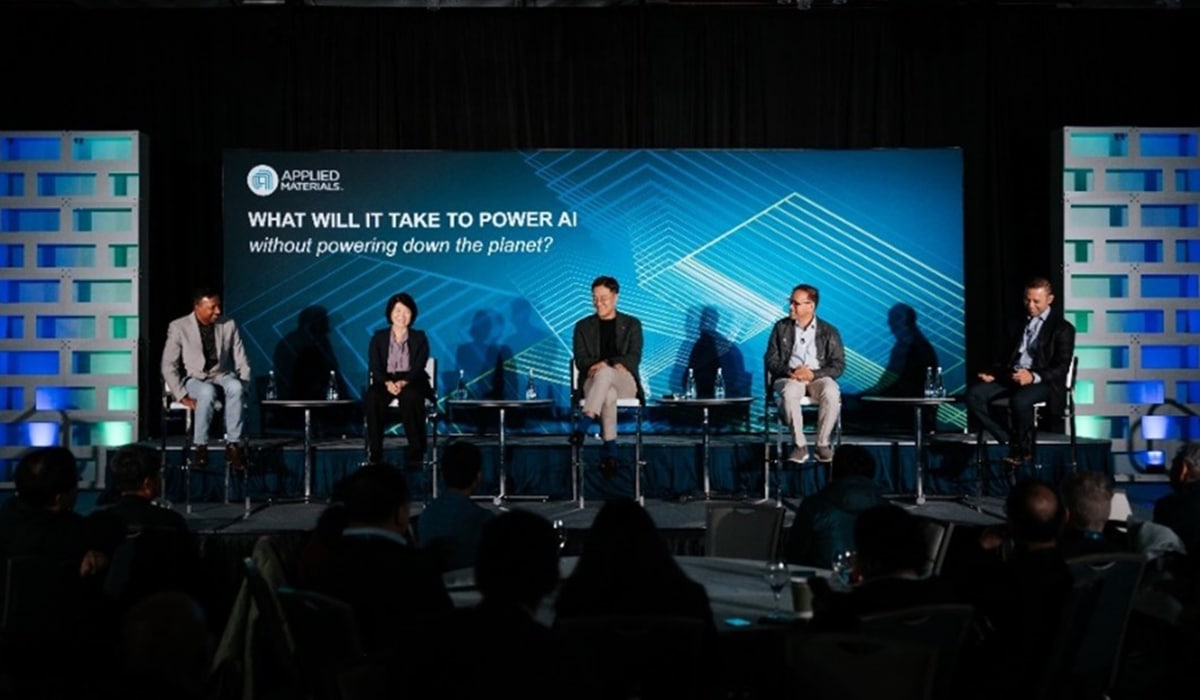
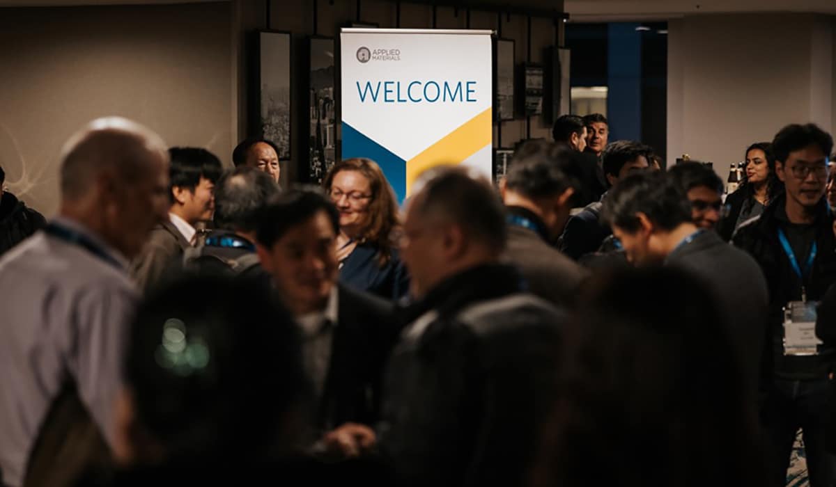
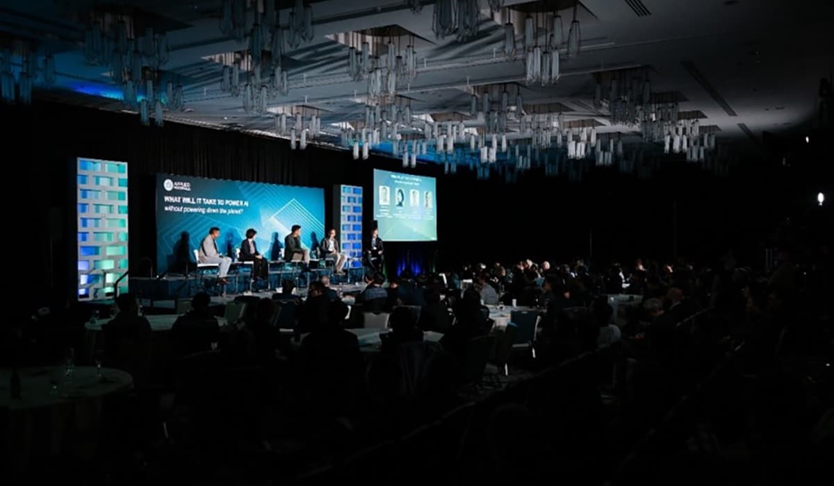
It’s the question that drew nearly 250 industry professionals to Applied Materials’ annual panel discussion during IEDM in San Francisco—an Applied tradition that has sparked industry-shaping conversations for more than a decade. AI promises extraordinary progress, from accelerating breakthroughs in medicine to unlocking new frontiers in science. But that promise comes with a steep price: a surge in resource demand rippling through every layer of infrastructure.
Against this backdrop, Applied Materials convened leading voices from Broadcom, SK hynix, Intel, and Applied—hosted by Dr. Kevin Moraes, Vice President of Strategy and Marketing for the Semiconductor Products Group—to tackle the energy wall head-on.
Data Movement—and Its Energy Toll
“The energy consumed by data movement between compute and memory is about 10,000 times bigger than actual computation,” said SK hynix’s Hoshik Kim, Senior Vice President & Fellow, Memory Systems Research, underscoring one of the biggest hurdles in AI infrastructure. That imbalance is only growing as “AI inference systems are scaling up and scaling out because they need more memory bandwidth and capacity.” Every boost in bandwidth means more data shuttling between compute and memory, driving energy consumption even higher.
The Need for Tighter Integration
Every millimeter of distance adds energy cost, which is why Broadcom’s Surendra Anubolu, Senior Technical Director and Distinguished Engineer, stressed: “Shorten the distance, and your orders of energy consumption can be reduced. If you could construct your system such that it can be fit into one package or one rack, then that gives you the best energy efficiency.”
That vision is already taking shape in today’s architectures. As Hoshik explained, “Near-memory computing is happening in the form of custom HBM—a critical, very essential component of AI infrastructure.” Applied’s Bala Haran, Vice President of Integrated Materials Solutions, also highlighted hybrid bonding as a pivotal advance in latency reduction: “It allows us to shorten the distance between components while consuming less power, and it works across multiple form factors—die-to-die, die-to-wafer, and wafer-to-wafer.”
Innovation Beyond Architectural Integration
Tighter integration cuts distance—but it introduces a new ceiling: thermal density. As Hoshik explained, “We’re pushing our HBM boundary toward 16-high, 20-high, even 24-high. But once you go beyond 16-high, thermal becomes a critical bottleneck. Our data center customers are increasingly concerned about heat dissipation at these heights.”
When packaging and stacking hit thermal walls, deeper material innovation is needed according to Intel’s Myung-Hee Na, Vice President and Semiconductor Technologist: “Gate oxide faces a scaling challenge, while the complexity of the nanosheet process also influences material choice. And we all know how difficult it is to change the channel materials. It takes a village—no, a whole country to make that happen.”
A New Materials Paradigm
Building on that reality, Bala outlined a two-horizon roadmap: “In the near term, enable nanosheet stacking and multiple generations of gate-all-around with low resistance, low capacitance, and advanced thermal materials. Longer term, if we want to sustain Moore’s Law and Dennard scaling, it has to be with disruptive materials.”
Myung-Hee underscored the complexity, noting that future materials must deliver not only heat dissipation but also robust electrical insulation: “We need a lower-k, thermally conducting, super dielectric that prevents leakage and breakdown issues.” While acknowledging the scale of the task, Bala remained optimistic: “It’s possible—it just needs a concerted effort through the ecosystem,” pointing to Applied’s EPIC platform as a catalyst for collaborative innovation with R&D partners across the value chain.
As Surendra reminded the audience, optimism has fueled past breakthroughs: “I remember a while ago, people were saying, ‘There's leakage everywhere. Nothing is going to work.’ But as an industry, we’ve come together with FinFETs and gate-all-around and turned the solution around.” He drew laughs with his quip: “I’m very, very hopeful—and I think my fellow panelists have a lot of responsibility to enable systems folks like me.”
Applied Materials is proud to help the industry tackle AI’s energy challenge through innovation in materials engineering, process technologies, and automation—and by championing collaboration that drives progress across the stack. To hear the full discussion, view the panel replay below.