Products & Technologies
Products & Services
Contact
Products & Services
Products & Technologies
Services
Resources
Contact

Stay updated on our content.
Applied Materials Convenes Industry Leaders on Advanced Patterning for the AI Era
March 24, 2026
If a leading‑edge chip were scaled to the size of a football field, many of its most critical features would be just one‑third the width of a blade of grass—yet the industry’s future depends on printing and controlling those patterns with extraordinary precision. The challenge intensifies as 3D architectural shifts, including Gate-All-Around (GAA) transistors, stacked DRAM/HBM, and advanced packaging, drive performance gains while dramatically increasing patterning complexity.
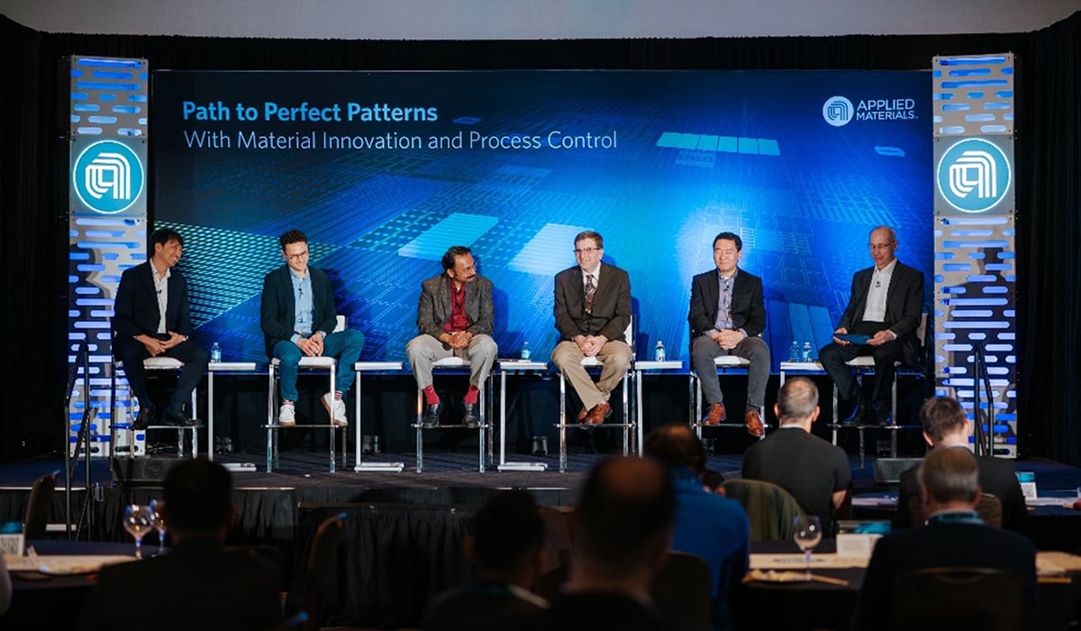
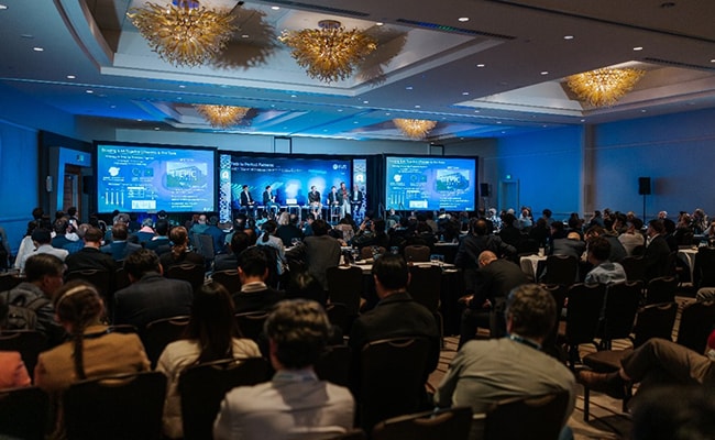
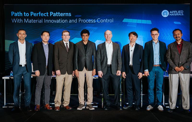
Alongside the SPIE Advanced Lithography + Patterning conference, Applied Materials convened an expert panel in San Jose, CA, focused on a central question of the AI era: How can the industry sustain patterning advances as demand for energy‑efficient performance accelerates? Moderated by Adam Brand, Applied Materials Vice President of EPIC Customer Technology, the discussion brought together senior leaders from JSR, imec, Intel, NVIDIA, and Applied Materials for a system‑level conversation before more than 300 attendees.

Balancing Pattern Fidelity with Scaling Economics
NVIDIA’s Da Yang, Senior Director of Product for Semi and EDA, observed that as the industry “reaches the angstrom regime,” a fundamental question emerges: how much further can we scale efficiently while keeping costs in check? The discussion quickly centered on lithography dosage—the energy used to print patterns—as it directly ties pattern quality to economics: while higher dose can improve fidelity, it typically reduces throughput and increases cost.
This tension underscored why dose efficiency has become a cross‑stack challenge. JSR’s Ken Maruyama, GM of R&D, explained that while photoresist technology has made major strides over the past decade, future dose targets exceed what resist advances alone can achieve, prompting a move toward broader ecosystem collaboration.
imec’s Frederic Lazzarino, R&D Manager of Novel Patterning Technologies, reinforced this view, noting that the stochastics and defects that result from dose reduction—such as line bridges and breaks—can be addressed through downstream recovery knobs. Panelists then raised several examples of such recovery approaches, including:
- Advanced etch: Applied Materials’ Siva Kanakasabapathy, Managing Director of Integrated Materials Solutions, explained how the Sym3™ Z Magnum™ conductor etch system improves etch‑depth micro‑balance, correcting dose‑driven variability without pattern distortion.
- Pattern shaping: Intel’s Curtis Ward, Principal Engineer, highlighted post‑processing to ease source‑design constraints, citing the Centura™ Sculpta™ patterning system for improving tip‑to‑tip spacing of critical dimensions and reducing variability.
Controlling Variation as a Key Performance Lever
As the discussion broadened to full‑flow co‑optimization, Da (NVIDIA) emphasized that at angstrom‑scale dimensions, even small variations can have outsized impact. Stronger variation control, he noted, helps the industry “get more bang for our buck”: eliminating just a few weak links can improve chip performance by ~1-2%—a meaningful gain when node‑to‑node advances stand at ~10-12%.
Building on that point, the panel aligned that sustaining pattern stability at scale will require tighter control loops, enabled by:
- AI-driven process control: Curtis (Intel) noted that AI/ML is accelerating advanced process control, enabling optimization down to the tool level.
- Advanced metrology: Frederic (imec) highlighted that shrinking pitches are outpacing traditional inspection, thus driving adoption of advanced 3D-profile characterization techniques such as cross‑section atomic force microscopy (AFM).
- Early collaboration: Siva (Applied) stressed that early engagement with customers and partners—through co‑innovation platforms like the EPIC Center—is critical for identifying the most crucial process parameters upfront, so deviations can be detected and corrected quickly.
Driving Patterning Innovation for the Angstrom Era
Advanced patterning in the angstrom era brings new challenges, but as Siva (Applied) observed, lithography has been predicted to “fall off a cliff” many times over the decades—and each time, the industry has pushed forward with fresh innovation. Ken (JSR) echoed this view, pointing to EUV’s progress from roughly 50nm pitch in 2009 to ~16nm today through sustained, cross‑ecosystem collaboration.
The panel agreed that delivering ideal patterns at future nodes will require deeper system‑technology co‑optimization and new models of ecosystem collaboration—areas where Applied has been investing for years. By convening leaders across the semiconductor value chain, Applied is enabling the alignment needed to keep scaling on pace with energy-efficient performance demands. Watch the full video replay below.