Products & Technologies
Products & Services
Contact
Products & Services
Products & Technologies
Services
Resources
Contact

Stay updated on our content.
Applied Materials Accelerates Materials Simulation for the AI Era in Collaboration with NVIDIA
March 16, 2026
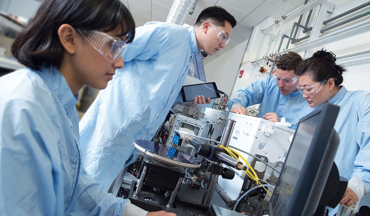
Late nights in the lab often start the same way: an engineer watching atomic-scale simulations inch toward an answer—Will this material work? As AI drives explosive growth in compute demand, that question is becoming far more urgent. Powering the AI era will require step-change gains in energy-efficient performance.
As the leader in materials engineering for the semiconductor industry, Applied Materials understands keenly that meeting this challenge requires understanding, evaluating, and optimizing materials faster—and with greater precision—than ever before. This imperative drives Applied’s collaboration with NVIDIA, where GPU-accelerated materials simulations are turning atomic-level insight into real-world innovation at greater speed.
Delivering Energy-Efficient AI with HfO₂
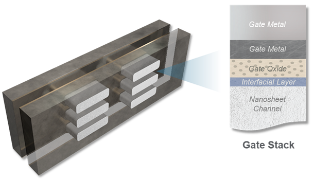
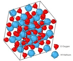
Few materials illustrate this challenge better than hafnium oxide (HfO₂). For more than a decade, HfO₂ has been the gold standard for the gate dielectric in high-k metal gate stacks. It extended transistor scaling by reducing leakage while maintaining performance—and remains foundational as the industry transitions to gate-all-around (GAA) transistors and next‑generation 3D architectures needed for energy‑efficient AI.
That performance, however, is defined by interactions invisible to the naked eye. Even angstrom‑level changes in structure, interfaces, or defects can have an outsized impact on power, performance, and reliability once a material is integrated into a device. Capturing these effects early—before a single wafer is processed—demands accurate, physics‑based materials simulation.
Modeling Molecules for Atomic-level Insight
Well before manufacturing, Applied researchers use materials simulations as part of their R&D process to evaluate a broad set of candidate dielectrics, interfaces, and material alternatives. After the right molecule has been identified, Applied must then enable reliable deposition of that material inside a vacuum chamber at manufacturing scale.
This requires precise control of complex chemical reactions, where numerous gas molecules interact with solid surfaces at atomic scale to form new materials. To optimize these reactions, Applied uses advanced reaction discovery techniques. These physics‑based simulations go far beyond chemical intuition, enabling engineers to identify pathways that reduce processing temperatures and limit impurities—both critical to yield, performance, and cost.
Surging Compute Demands in Materials Simulation
Just one step in a multi-stage chemical process can require up to thousands of reaction pathway searches—essentially stress‑testing all possible reaction routes to find the most efficient one. To support this work, density functional theory (DFT) serves as the industry standard for materials simulation—simplifying complex quantum mechanics and enabling tractable predictions of electronic behavior.
Historically executed on CPUs, DFT simulations are highly compute‑intensive, often requiring hours to days—and in some cases weeks or more—to complete. These long runtimes force scientists to reserve high‑accuracy methods for only small to modest system sizes, limiting their adoption in large-scale industrial workflows.
Accelerating Materials Simulation with GPU Compute
That’s where Applied’s collaboration with NVIDIA comes in. NVIDIA recently introduced cuEST, a CUDA-X library that shifts core electronic-structure calculations onto GPUs. By accelerating the most demanding steps of the DFT modeling process , cuEST significantly reduces simulation time while preserving the required accuracy.

Integrating cuEST into simulation workflows dramatically shortens evaluation and optimization cycles. For assessing material candidates, a typical simulation that once took five days on 64 CPU cores now completes in 2 hours on an NVIDIA B200 GPU. At the next stage, a reaction discovery run of ~15,000 pathway searches on 400 CPU cores—previously taking 1.5 weeks—can be completed in just 5 hours on an NVIDIA B200 GPU.
These 55x accelerated simulations unlock a much broader design space, allowing teams to evaluate more material candidates and probe deeper, more complex reaction networks. The result is faster iteration and earlier convergence on optimal solutions.
As lithography-based scaling delivers diminishing returns, performance gains increasingly hinge on materials engineering—new dielectrics, semiconductors, and interfaces within complex 3D device architectures. In this environment, fast and high-fidelity materials simulations are more critical than ever to sustaining innovation.
Advancing Energy-Efficient AI with High Velocity Co-Innovation
This collaboration with NVIDIA exemplifies Applied’s strategy of high-velocity co-innovation, enabled globally through the EPIC platform. By engaging early and working in parallel with customers, partners, and academia in a secure environment, Applied gains deep visibility into customer roadmaps to better guide R&D investments. At the same time, partners gain early access to Applied’s R&D portfolio—accelerating learning, validation, and impact on both sides.
That speed matters. Bringing a technology from research to high-volume manufacturing typically takes 10 to 15 years—but AI’s energy challenge can’t wait, and no company can solve it alone. By combining Applied’s materials expertise with NVIDIA’s cuEST‑enhanced computing, this collaboration moves electronic structure modeling from the lab to the fab—transforming fundamental science into energy‑efficient technologies that power the devices we use every day.