Products & Technologies
Products & Services
Contact
Products & Services
Products & Technologies
Services
Resources
Contact
Posted
February 18, 2026
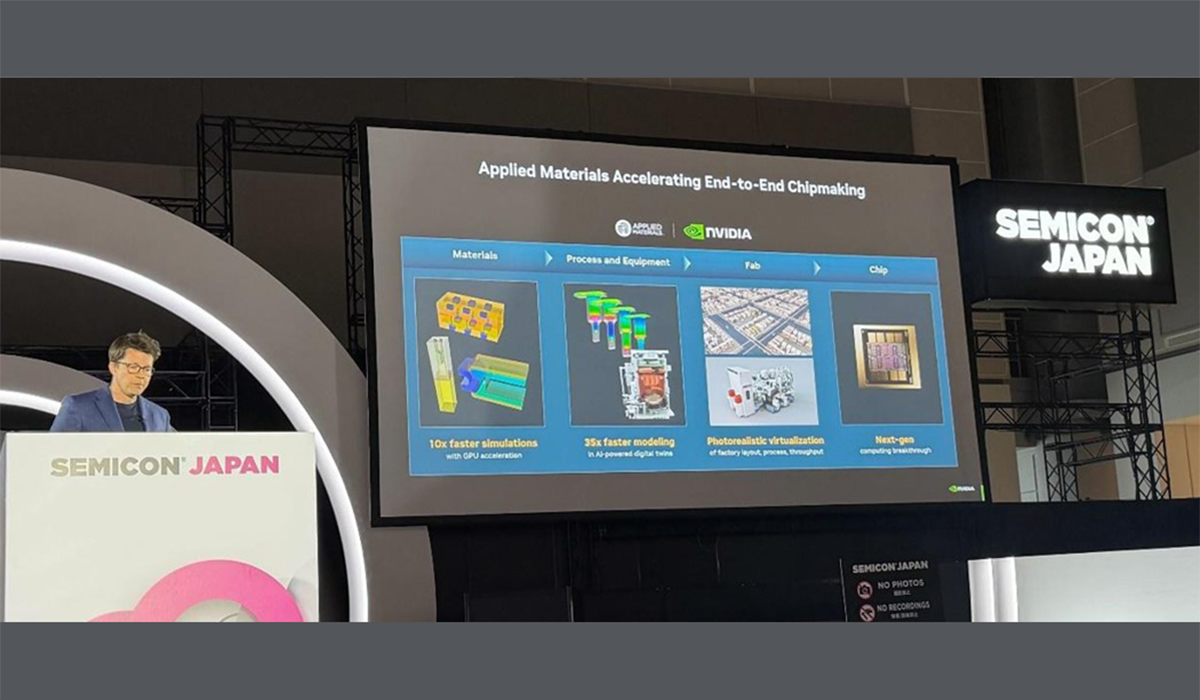
Applied Materials Collaborates With NVIDIA to Accelerate End-to-End Chip Manufacturing
A New Era Begins
Momentum around AI‑driven semiconductor manufacturing has never been stronger. At recent industry events, Timothy Costa, NVIDIA’s GM for Industrial & Computational Engineering, highlighted how Applied Materials is teaming up with NVIDIA to revolutionize the AI infrastructure production journey.
This collaboration comes at a pivotal moment for the semiconductor industry. As chips become more advanced, manufacturing processes have grown exponentially more complex – rendering traditional modeling too slow for the rapid innovation cycles demanded by AI and other data-intensive applications. Applied is collaborating with NVIDIA to tackle this challenge with a new paradigm that makes chip manufacturing faster, more reliable, and cost-effective from end to end.
Building from the Atomic Level
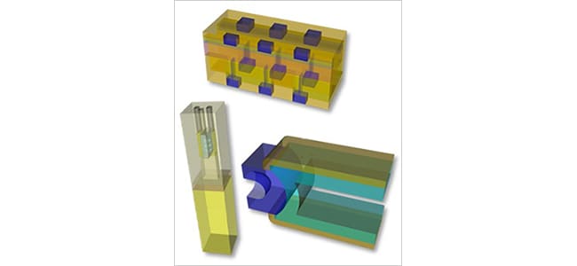
Every chip breakthrough starts with the smallest building block: materials. Applied’s Ginestra software simulates material behavior at the atomic level, providing insights into electronic properties and interactions that help optimize semiconductor device performance. Traditionally, such simulations could take weeks – but with NVIDIA AI infrastructure and NVIDIA accelerated libraries, including NVIDIA CUDA-X Direct Sparse Solver, cuDSS, Ginestra now accelerates computations up to 10x faster than CPU-only runs. These virtual experiments let engineers evaluate thousands of material combinations without costly physical trials, dramatically reducing time and expense before a single wafer is processed.
Engineering the Process
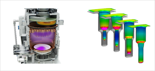
The next challenge is predicting how thousands of process steps interact to shape semiconductor device performance. Applied’s ACE+ multi-physics suite models complex phenomena—such as fluid flow, heat transfer, plasma, and electromagnetics—to enable virtual chamber prototyping and optimization of hardware and process recipes. Now, with NVIDIA AI infrastructure, ACE+ topography simulations can run up to 35x faster—compressing weeklong studies into same-day results. Building on that speed, the NVIDIA PhysicsNeMo framework converts ACE+ data into real-time digital twins, allowing engineers to adjust parameters and get near-instant feedback.
Scaling to the Fab
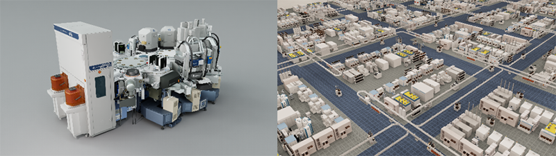
With process refinements validated digitally, Applied brings them to life on an Integrated Materials Solution based on the Endura™ platform – combining seven advanced technologies under vacuum to deliver the atomic-level precision essential for chipmaking. The focus then shifts beyond individual tools to the entire factory, as Applied uses NVIDIA Omniverse libraries to create photorealistic, interactive digital twins of full-scale fabs. Teams leverage these virtual environments for fab planning and operations – simulating equipment layout to maximize output and space, analyzing throughput to remove bottlenecks, and fine-tuning process control to boost yield before implementation.
Powering Next-Generation Computing
Semiconductor complexity is surging – from angstrom-level control in transistors to multi-die packaging and factory-wide variability. By combining high-fidelity physics with GPU-accelerated AI from NVIDIA, Applied Materials is compressing R&D cycles, improving yield, and supercharging innovation across the industry. For chip manufacturers, this means faster iteration, more predictable scale-up, and improved economics over the product lifecycle. Ultimately, this collaboration marks a transformative leap toward next-generation computing – where AI accelerates AI, from atoms to fabs.
See It in Action
Explore how Applied Materials is accelerating end-to-end chipmaking with NVIDIA. Watch the demo video here: