Products & Technologies
Products & Services
Contact
Products & Services
Products & Technologies
Services
Resources
Contact
Posted
December 20, 2024
Advanced Packaging Enters a New Dimension
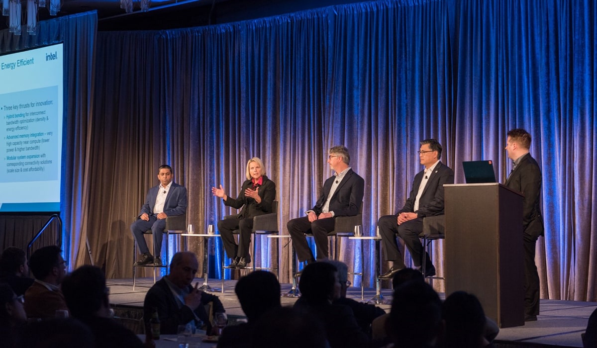
For more than a decade, Applied Materials has hosted a technical program alongside the IEEE International Electron Devices Meeting (IEDM) – the premier conference on leading-edge semiconductor technology. For this year’s program, we brought together some of the industry’s brightest minds to discuss the future of chip packaging in the AI era. Moderated by prominent industry analyst and YouTube educator Dr. Ian Cutress, the panel featured experts from AMD, Intel, Cadence and Applied.
Driven by an insatiable appetite for data, AI is introducing a new set of demands to the semiconductor roadmap. As traditional 2D scaling has slowed, innovation in 3D architectures has accelerated across multiple vectors – from the device to the system level. Perhaps the biggest impact has been in advanced packaging, which creates entirely new opportunities for volumetric scaling through heterogeneous integration.
Key takeaways: Now that the first 3D packaged systems are on the market, what will it take for the industry to move “beyond 3D” and enable the true potential of AI? Several key themes emerged from the thought-provoking discussion as our panelists debated the question, "3D Is Here, Now What?":
- Panel moderator Ian Cutress discussed the changing nature of Moore’s Law. While long viewed as a statement about transistor density and economics, in the AI era it now revolves around putting as many transistors as possible in a single-packaged system. “We have companies out here talking about aspiring to one trillion transistors by 2030 – enabled through advanced packaging and 3D techniques.”
- AMD’s Deepak Kulkarni highlighted three key vectors for packaging innovation – 3D multi-tier stacking, 2.5D panel-level packaging and co-packaged optics. “In all of these, there is a significant drive towards energy efficiency,” he said. “We don't want to just pack compute and memory for the sake of packing it. We want to make it energy efficient by bringing all of these components as close to each other as possible. Energy efficiency is a big driver for what comes after 3D.”
- Intel’s Johanna Swan emphasized the importance of interconnect scaling with hybrid bonding to manage the power demand from AI. “Hybrid bonding is out there at a certain scale today in some products – just below 10 microns – but I certainly think it’s going to continue to scale below one micron,” she said. “That’s really going to help drive the density that’s needed to drop the energy.”
- Kam Kittrell from Cadence described the growing need for thermal management through design techniques and new materials. “When you were doing a 2D chip, the thermal was a last-minute check,” he said. “Now whenever you’re stacking the chips and putting them all in one single package, the heat evacuation is very difficult, and the heat can give you runaway thermal effects. It’s very difficult to stack these chips too high because the heat will rise up to the top, and the top chip will be hotter than all the rest.”
- Applied’s Terry Lee discussed the need to collaborate across the ecosystem to accelerate the roadmap and bring new technologies to volume production at a faster rate. “When you look at things like hybrid bonding, we’re actually trying to bring the front-end tool capabilities into the packaging space,” he said. “The idea is, how do you put together dissimilar chips in an environment where we can improve productivity, reduce queue time and defectivity, and put it all together in one system to improve yield and productivity for our customers.”
More context: Here is a video replay of the entire discussion:

A picture is worth a thousand words: Below is a selection of photos from the panel.

Ian Cutress, Founder and Chief Analyst, More Than Moore
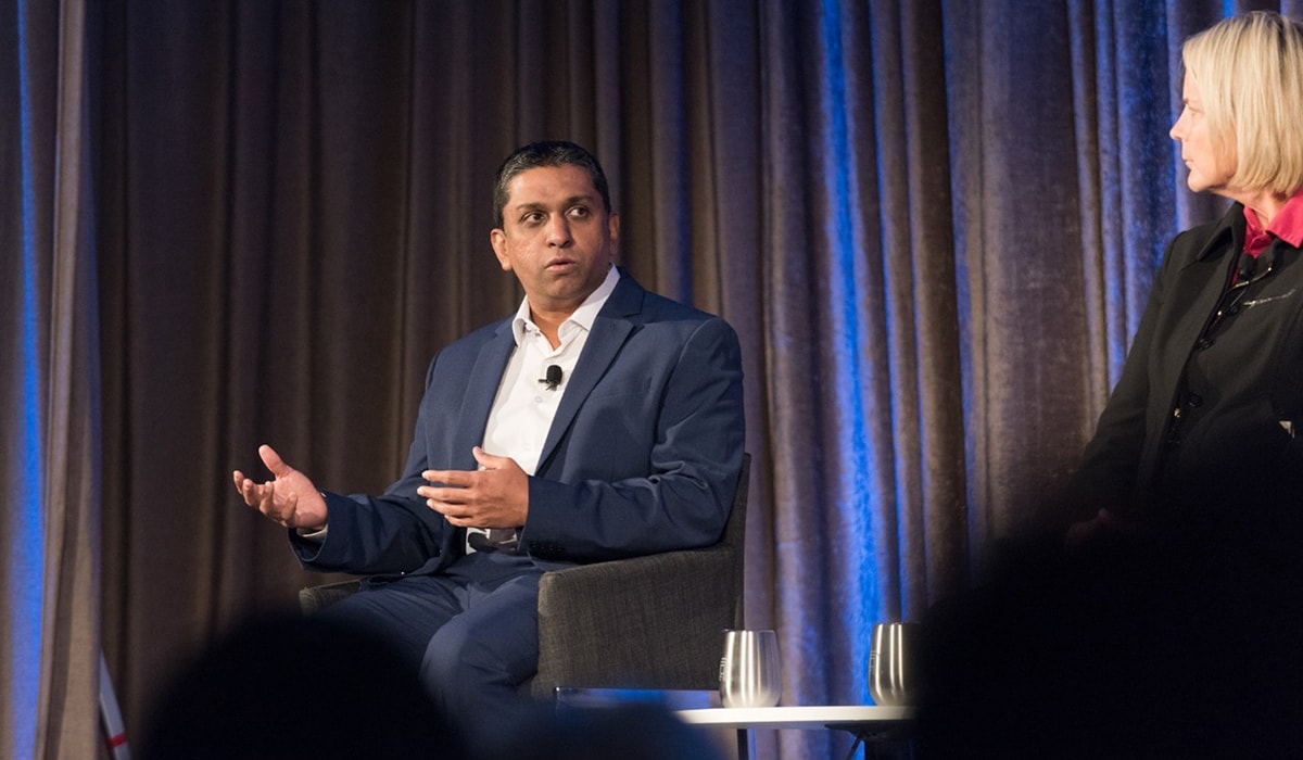
Deepak Kulkarni, Senior Fellow, Advanced Technology Integration, AMD
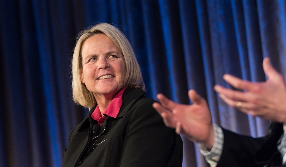
Johanna Swan, Fellow, Director of Package Research and Systems Solutions, Intel

Kam Kittrell, Vice President, Product Management, Digital Signoff Group, Cadence
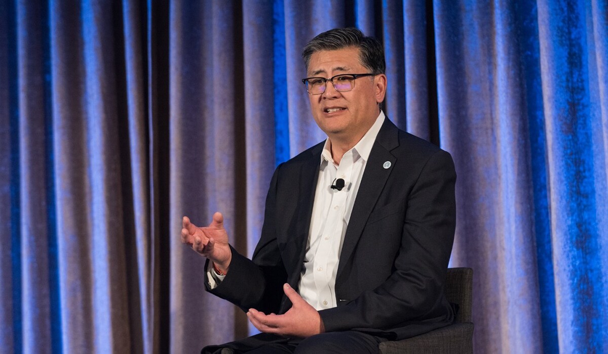
Terry Lee, Vice President and General Manager, Heterogeneous Integration Business, Applied Materials
- 1 / 5
- 2 / 5
- 3 / 5
- 4 / 5
- 5 / 5