Products & Technologies
Products & Services
Contact
Products & Services
Products & Technologies
Services
Resources
Contact
Posted
February 05, 2026
A New Chapter for Applied Materials India
What’s New
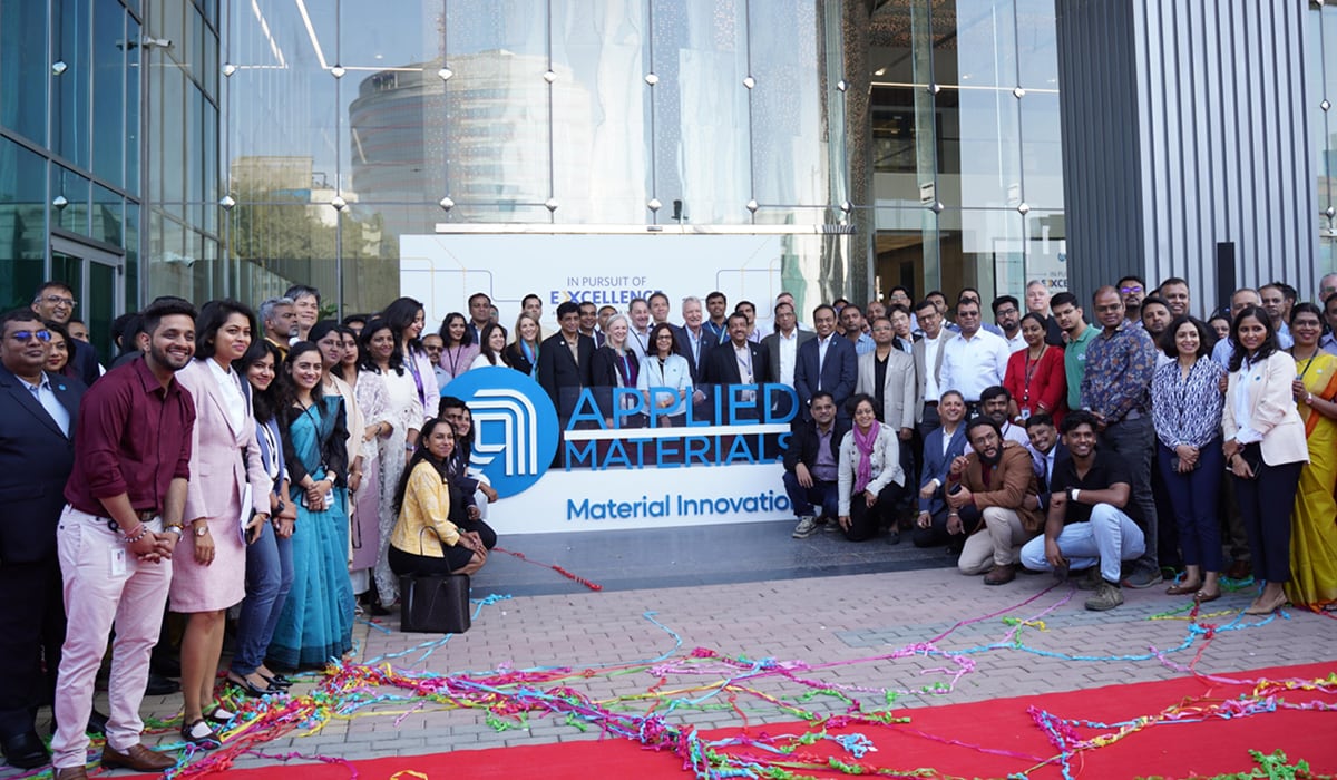
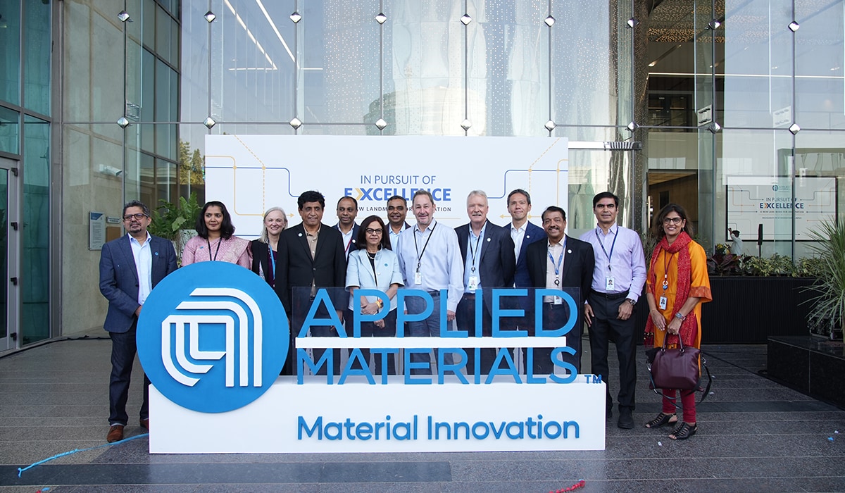
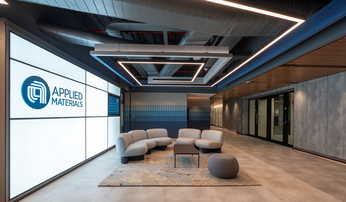
We recently held an inauguration ceremony for our new 8 lakh+ (800,000+) sq. ft. campus in Bengaluru — it was a moment filled with pride, excitement, and shared accomplishment for Applied Materials India. The new building represents how far we’ve come and how deeply we’re invested in shaping India’s semiconductor future — a reminder that our greatest strength is our people and the innovation we create together.
A Milestone Moment
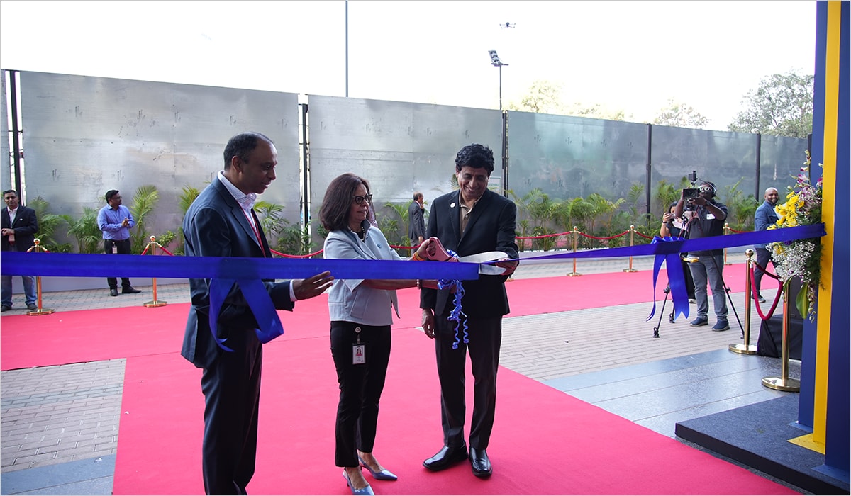
The day began with a ribbon cutting ceremony led by Prabu Raja, President of Applied’s Semiconductor Products Group, Joji Gill, Senior Vice President and Chief Human Resources Officer, and Avi Avula, President of Applied Materials India. We were also honored to welcome Ms. Gunjan Krishna (IAS), Commissioner for Industrial Development & Director, Department of Industries & Commerce, Government of Karnataka. Her presence, alongside our global leadership, underscored Applied’s growing role in strengthening India’s semiconductor and advanced technology ecosystem.
Avi captured the spirit of the day: “Our new campus is more than a building — it is a symbol of what Applied Materials India stands for. It reflects our passion for innovation, our commitment to excellence, and our belief in the power of our people. This campus will inspire new ideas, new collaborations, and new breakthroughs that shape the future of semiconductors.”
Technology Meets Creativity
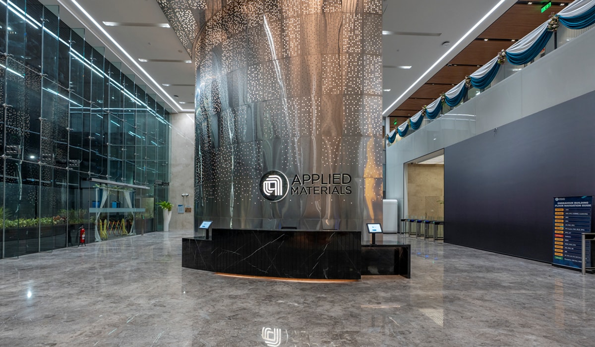
The new campus in Bengaluru is built to be a space where technology meets creativity. Art and technology are central to the building’s design and guide everyday movement throughout the space. A three-dimensional “Sand to Silicon” installation anchors the ground floor, introducing our materials engineering story. Curated installations throughout the building feature rare and diverse Indian art. This seamless integration between technology and culture is meant to foster collaboration and innovation as our teams work to accelerate R&D and deepen industry and academic partnerships.
Building From a Strong Foundation
The opening of Applied’s new workplace in Bengaluru builds on more than 20 years of success in India. Our key capabilities here include the India Validation Center—the country’s only facility capable of processing 300mm wafers—which is a key hub for semiconductor equipment product design, simulation, testing, and validation, along with a clean-room facility for high-precision inspection, prototyping, and component qualification. These are complemented by the AI Center of Excellence in Chennai, where advanced analytics and AI are used to support high-volume manufacturing through automation, improve throughput, and refine equipment design. Together, these facilities and capabilities, including the new campus in Bengaluru, underscore Applied Materials’ commitment to be an integral part of strengthening India’s semiconductor ecosystem.
- 1 / 4
- 2 / 4
- 3 / 4
- 4 / 4