Products & Technologies
Products & Services
Contact
Products & Services
Products & Technologies
Services
Resources
Contact

Stay updated on our content.
Unlocking Next-Gen AI Chips Through Advanced Materials Modification
Apr 2, 2026
By Andy Lo

Imagine driving the world’s premier sports car down a road riddled with potholes. The engine may be incredibly powerful, but the road beneath it limits how that power translates into speed.
The same is true for today’s most advanced AI chips. At leading-edge nodes, chipmakers are packing five distinct materials into a space roughly 1/10,000th the width of a human hair. Even atomic level roughness feels like a major pothole to electrons, slowing signals, increasing resistance, and reducing energy efficiency. That’s why materials engineering has become more critical than ever.
The Rise of Materials Modification
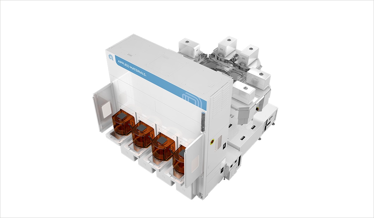
Materials modification has long been a core pillar of semiconductor manufacturing, and its importance has only grown in the AI era. Today, it’s a multi‑billion‑dollar materials engineering segment, fueled by chipmakers’ need for advanced treatments that precisely condition surfaces and interfaces after deposition—and an area where Applied Materials leads. Producer® Viva™, Applied’s radical treatment solution, is designed for the nanoscale regime and enables chips to be engineered atom by atom for high performance at scale.
Built on Applied’s high‑throughput Producer platform, Viva combines gentle chemical radicals with precisely controlled heat in an ultra‑clean environment. Designed for high‑volume manufacturing, its multiple twin‑wafer chambers deliver efficient, cost‑effective processing across both front‑end‑of‑line (transistor) and back‑end‑of‑line (wiring) applications.
Enabling the Next Generation of Transistors
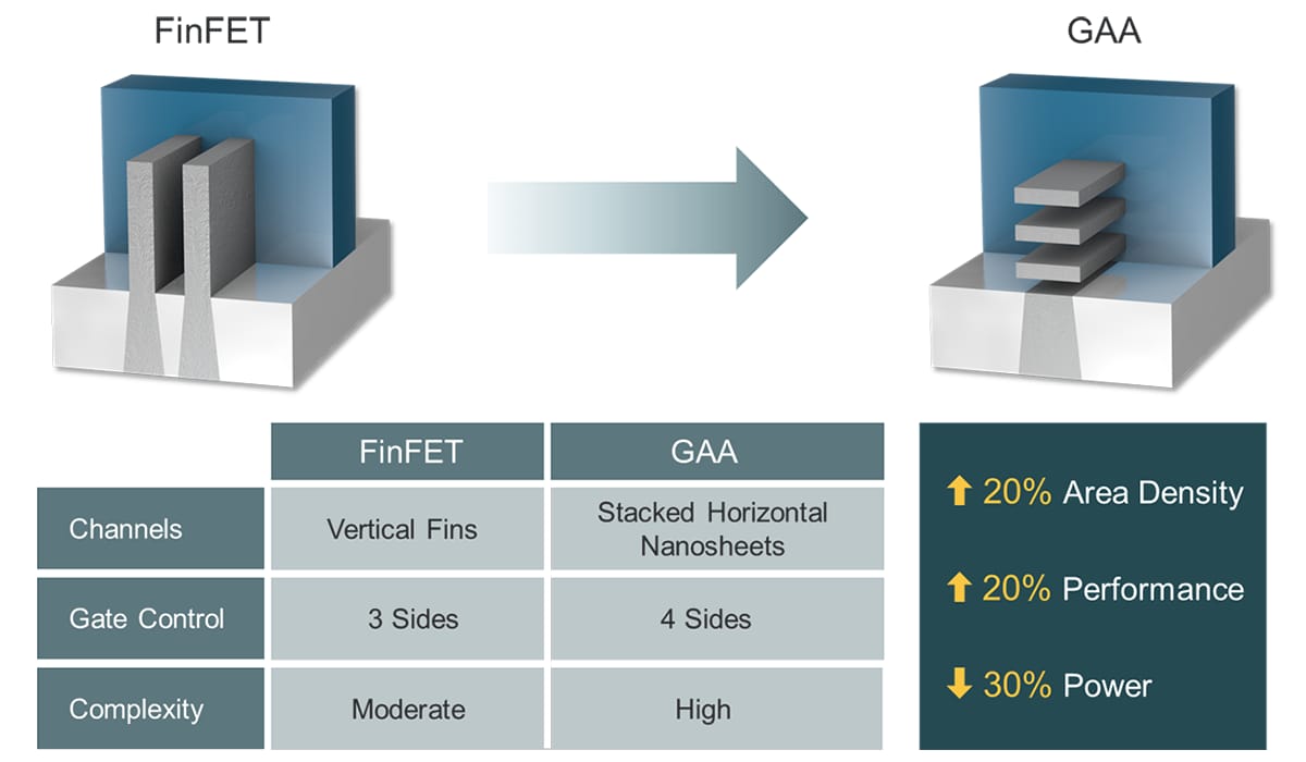
One of Viva’s most compelling applications is in gate‑all‑around (GAA) transistors, the next‑generation architecture succeeding FinFETs. GAA devices deliver higher performance and lower power, but they also demand far greater materials precision.
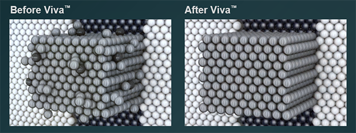
GAA transistors rely on ultra‑thin silicon nanosheets that must be exceptionally smooth and pristine. Even angstrom‑level roughness or residue can increase interface defects, trapping electrons and degrading current flow. Conventional smoothing solutions require very high temperatures or aggressive processes. However, excessive heat can damage delicate GAA layers or drive unwanted diffusion of impurities deep into the silicon channel, while aggressive treatments risk removing too much silicon from the current-carrying channels.
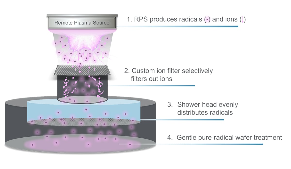
Viva addresses these challenges with a patented radical‑based approach that delivers only pure hydrogen radicals to the wafer, filtering out high‑energy ions that can cause plasma damage. The radicals absorb into the silicon and lower its surface energy (similar to reducing tension). This allows atoms at the interface to move and be rearranged into a smoother structure—much like softening fabric so wrinkles can be ironed out easily.
Crucially, Viva’s wide temperature range—about 150°C to 650°C—supports low‑thermal‑budget processing while preserving flexibility for higher‑temperature treatments as needed. The result is uniform, damage‑free smoothing that yields clean, defect-free interfaces and tighter electrical control. Together, these gains are powering faster, more efficient GAA transistors at leading chipmakers.
Reducing Resistance in Advanced Wiring
Viva also plays a critical role in chip wiring at advanced nodes. Copper is made up of many tiny crystal grains, and at the interfaces between them—called grain boundaries—electrons scatter and lose momentum, much like hitting speed bumps. As wires shrink, grains get smaller, grain boundaries multiply, and resistance rises. Moreover, small amounts of dopants such as manganese are added to maintain reliability in these narrow wires, but they can add resistance if not carefully engineered.
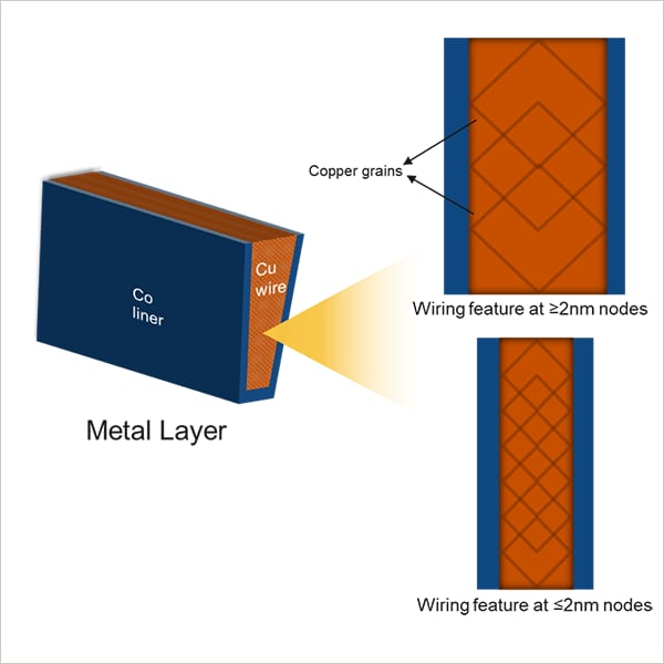
By treating the copper immediately after deposition, Viva tackles both challenges simultaneously to optimize performance. Hydrogen radicals promote larger copper grain growth, reducing grain boundaries and improving electrical flow. At the same time, they drive manganese to the copper surface where it enhances reliability, rather than leaving the dopant in the bulk metal where it might raise resistance.
Viva then applies a precise thermal anneal to further enhance dopant segregation and grain growth. When co-optimized with Applied’s Endura® platform’s copper deposition, Viva delivers more than a 30% reduction in copper resistance at 2nm and beyond, unlocking meaningful gains in overall chip performance.
Extending Beyond Logic into Memory
While Viva is seeing strong traction in leadin-gedge foundry/logic, its flexible architecture also makes it highly relevant in memory. As DRAM device structures become increasingly logic-like and wiring-intensive, many of the same materials challenges are coming to the forefront—driving the need for advanced materials modification.
Well positioned to support next-generation memory and logic designs, Viva expands Applied’s industry leadership in treatment solutions that help chipmakers smooth the road so the world’s most advanced chips can perform to their full potential.
Learn more about Viva and other leadership technologies in Applied’s portfolio at our Logic Master Class on April 8 at 9am PT.
Andy Lo
Head of Strategy and Marketing, FEP

Andy Lo is the Head of Strategy and Marketing for FEP (Front End Product) BU at Applied Materials, responsible for the unit’s gross margin, market share growth, and product commercialization. Andy joined the semiconductor industry in 1996 and has held various positions at Applied Materials since 2000, including PSE, BM, PSE Manager and GPM, working across Ion Implantation, Epitaxy and FEP technologies.