Products & Technologies
Products & Services
Contact
Products & Services
Products & Technologies
Services
Resources
Contact
Posted
September 09, 2025

Stay updated on our content.
The ecoUP™ Portfolio: Paving the Path to a Sustainable Future

by Hongtao Liu and Vyasa Shastry
The semiconductor industry is at the forefront of technological innovation, but it also faces significant environmental challenges. Hyperscalers – the giants of data processing, storage and consumer devices – have set ambitious targets to achieve Net Zero carbon emissions by 2030. Given the profound impact of semiconductor devices in our daily lives, this goal is not just a corporate responsibility but a necessity for the planet's future. The path to Net Zero involves accelerating grid decarbonization and reducing energy consumption and greenhouse gas (GHG) emissions of semiconductor manufacturing, which presents opportunities for innovation and new green solutions.
Semiconductor manufacturing is a highly complex and energy-intensive process. Therefore, achieving Net Zero involves optimizing every aspect of a chipmaker’s fab, from the facility’s HVAC system to the chamber gas panels, from recipe optimizations to smart software, and incorporating green components (e.g., heaters, RF bias, turbopump, chillers, etc.). Equipment makers, along with others in the supply chain, play a crucial role in enabling reduction of equivalent energy consumption and direct emissions of a semiconductor fab.
Applied Materials' Commitment to Sustainability
At Applied Materials, we are committed to reaching our "3 by 30" goals, which aim to support our customers’ sustainability targets. Our comprehensive strategy addresses energy consumption and emissions at both the chamber and subfab levels. Specifically, we target a 30% reduction in equivalent energy consumption, a 30% reduction in chemical consumption, and a 30% decrease in footprint by 2030 (from 2019 baseline).
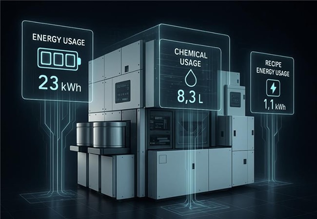
In 2020, we made a bold commitment to build an ecoUP™ portfolio of products and services, and, today, we are excited to announce the release of our ecoUP Vantage™ Radiance™ RTP system and ecoUP RadOx™ RTP on both the Vantage and Centura™ platforms. The Radiance RTP system is used for atmospheric applications like dopant activation and silicide formation, while the RadOx system is used for critical reduced-pressure oxidation steps like memory gate oxide and shallow trench isolation liner oxide. The ecoUP versions are designed to offer significant improvements over their original counterparts, including up to 20% savings on total energy consumption, advanced thermal management, reduced chemical usage, and improved process uniformity, all contributing to a lower environmental impact.
We are also thrilled to announce that our industry-leading Endura™ CuBS (Copper Barrier/Seed) RF XT PVD system has been optimized for energy savings with green components. The cumulative savings from these improvements result in approximately 10% less equivalent energy consumption, setting a new benchmark for energy efficiency in the industry. The system serves logic and memory applications at the 32nm/28nm nodes and beyond, featuring high-ionization PVD technology for low-temperature film deposition with minimal overhang and smooth morphology, along with advanced thermal management and reduced chemical usage.
Our solutions not only reduce energy usage but also enhance the overall operational efficiency – and lower operational costs! – of semiconductor fabs. At Applied, we use a systems approach to address the chipmaker’s sustainability challenge. Unlike fragmented approaches, our solutions span across multiple processes (e.g., PVD, CVD, ALD, etch, etc.), accelerating learning and unlocking greater optimizations and operational efficiencies. This holistic approach positions our customers for long-term success in a competitive landscape.
Collaborative Efforts for a Sustainable Future
The journey to Net Zero involves every player in the value chain, from hyperscalers and chipmakers to equipment manufacturers and material suppliers. Each has a role to play in reducing Scope 1, 2, and 3 emissions. Hyperscalers are investing heavily in renewable energy to reduce their carbon footprint, while chipmakers are deploying green solutions across their fabs. Similarly, equipment and chemical manufacturers are developing green innovations across their product portfolio. This underscores the importance of collaborative efforts to achieve sustainability goals across the semiconductor supply chain. At Applied Materials, we are committed to leading these collaborative efforts and working with our partners to accelerate the path to Net Zero.
Hongtao Liu
Strategic Marketing Director, FEP

Hongtao Liu is the Strategic Marketing Director in the Front-End Products group at Applied Materials. She has over 20 years of experience in Product Marketing, Business Management and Application Development Engineering in the Semiconductor Equipment Industry. Hongtao obtained her Ph.D. in Chemistry from UC Irvine.
Vyasa Shastry
Senior GPM, MDP-ALD

Vyasa Shastry is a Senior GPM in the MDP-ALD Group at Applied Materials. He has an MBA from Kellogg. During his PhD (in materials engineering) at IISc Bangalore and Imperial College London, he worked on industrial research problems for Rolls Royce, Boeing, and GM. He brings over 10 years of experience spanning Product Management, Strategy, Business Development, and Entrepreneurial ventures. Prior to joining Applied, Vyasa worked across Private Equity, Consulting, and Startups.