Products & Technologies
Products & Services
Contact
Products & Services
Products & Technologies
Services
Resources
Contact

Stay updated on our content.
Precision from the Bottom Up: Enabling Angstrom-Era AI with Sym3™ Z Magnum™
Feb 26, 2026
By Somit Joshi

Picture an elevator shaft running through a towering skyscraper. The higher the number of floors, the more critical it is that the shaft stays plumb, precisely dimensioned, and level at every landing. Minor alignment or stability errors quickly compound as the structure grows—turning height from a benefit to a liability.
Advanced chipmaking faces a similar challenge. As traditional 2D Moore’s Law scaling slows, the transistors and memory cells needed for expanding AI workloads increasingly come from vertically stacked semiconductor devices—as with gate‑all‑around (GAA) transistors and high‑bandwidth memory (HBM) DRAM. To enable this vertical integration, chipmakers must be able to etch extremely deep, narrow 3D trenches through multiple layers to build and connect logic, memory, and wiring.
Setting the Gold Standard for 3D Etch Precision
Extremely high-aspect-ratio features demand uncompromised geometric control, as even small variations in depth, sidewalls, or bottom shape can cascade into switching variability, leakage, reliability loss, and yield failure. As we continue to scale, etch precision becomes a decisive lever. To surpass the limits of traditional RF‑based etch control, Applied debuted a revolutionary Pulsed Voltage Technology (PVT) in 2025 with the release of Sym3™ Z—the newest member of the Sym3 conductor etch family.
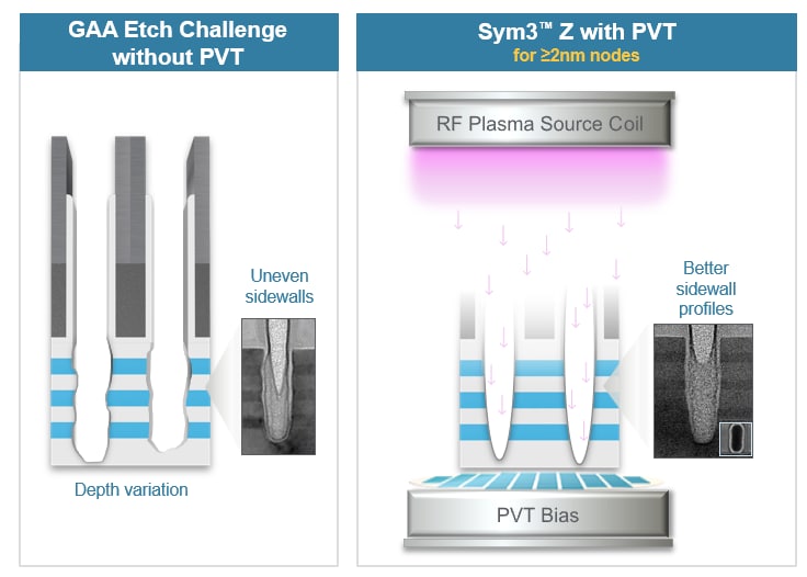
By operating at microsecond timescales instead of RF’s millisecond pulses, PVT offers far sharper control over ion formation and impact at the wafer surface. As aspect ratios climb, the result is smoother sidewalls and more uniform vertical profiles. With tool‑of‑record status in 2nm logic and HBM DRAM manufacturing and more than 250 chambers deployed, Sym3 Z sets a new baseline for advanced 3D conductor etch patterning.
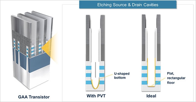
Still, looking ahead to future nodes, scaling pressures continue to intensify. As the industry enters the angstrom era, 3D structures are growing deeper and must meet ever‑tighter tolerances—requiring perfectly flat, rectangular bottoms and uniform feature depths across the wafer.
Raising the Bar for Scaling in the Angstrom Era
To meet these exacting requirements, Applied recently launched the Sym3™ Z Magnum™ conductor etch system. Purpose-built for angstrom‑level 3D patterning, Magnum extends the proven Sym3 Z platform by bringing plasma and ion control closer to the wafer than ever before.
At the core of Sym3 Z Magnum is PVT2, the second generation of Pulsed Voltage Technology. PVT2 concentrates reactant ions directly at the wafer surface, allowing etched features to respond more predictably to process settings as depths increase. Crucially, it enables near‑wafer plasma control alongside independent tuning of ion angle and ion energy. The result is a dual‑mode etch that combines rigorous trench etching and precise bottom‑corner shaping. This simultaneous delivery preserves feature geometry even as aspect ratios climb and tolerances narrow. Where conventional etch systems trade off plasma proximity and ion directionality, Sym3 Z Magnum is the first to offer both—closing a critical gap for next‑generation 3D architectures.
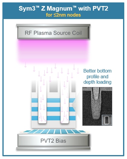
To amplify the benefits of PVT2, Sym3 Z Magnum adds plasma source enhancements that optimize the overall process environment—from reactant generation to byproduct evacuation. The new source extends reactant exposure by 10x, enabling complete adsorption at the bottom of high‑aspect‑ratio features and thus improving depth uniformity. Together with PVT2, this capability gives chip manufacturers tighter control of feature geometry across the wafer.
Turning Next-Generation AI Roadmaps into Manufacturable Reality
As GAA logic and HBM DRAM architectures push deeper into silicon, performance per watt increasingly hinges on the fidelity of the smallest, deepest features. The future of AI computing is 3D—and Sym3 Z Magnum equips logic and memory chipmakers to master angstrom-level patterning at scale.
Somit Joshi
Managing Director of Marketing, Etch

Somit heads the Strategy & Product Management team in Applied’s Etch business unit, where he is responsible for driving the product strategy and strategic planning for upcoming industry inflections. Somit has more than 25 years of experience in the semiconductor industry across both device makers and OEM providers. He holds an MBA in product management and an MS in materials science.