Products & Technologies
Products & Services
Contact
Products & Services
Products & Technologies
Services
Resources
Contact
Posted
February 03, 2026

Stay updated on our content.
Future of Advanced Packaging: Industry Insights on Co-Innovation and Talent Development
By Kevin Moraes
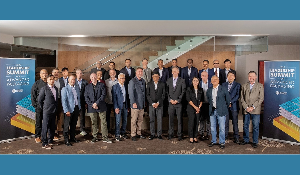
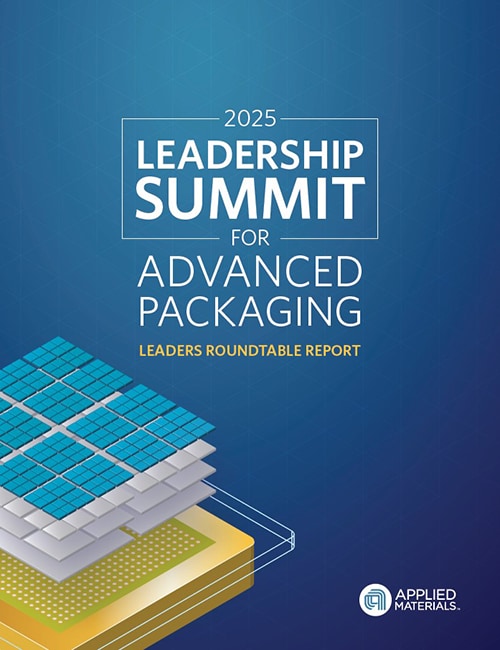
Innovation thrives on technology and talent—a principle that shaped our second annual Leadership Summit for Advanced Packaging held in Phoenix, Arizona. At the heart of the event was the Leaders Roundtable, where visionaries from across the semiconductor ecosystem gathered to share bold approaches for the future. These discussions centered on two themes driving the industry forward: Collaboration Across Boundaries and Workforce Development. I’m excited to share our report highlighting the key insights that will help turn vision into reality in 2026.
Collaboration & Integration: Breaking Down Silos
Traditionally, semiconductor companies kept their roadmaps under wraps to protect competitive advantage. But advanced packaging has changed the game, demanding an unprecedented level of integration that no single organization can tackle alone. Recognizing this, Dan Hutcheson, Vice Chair and Senior Research Fellow at TechInsights Inc., facilitated a roundtable on how collaboration can fuel the next wave of progress and why transparency, even among competitors, creates value for all.
“Success comes from the ability to partner broadly while maintaining deep expertise in some areas and a broad understanding of how your work impacts others.”
— Glenn Daves, Senior Vice President of Package Innovation, NXP Semiconductors
Participants agreed that collaboration must span both vertically and horizontally—connecting every layer of the value chain and bridging companies and disciplines. The discussion examined strategies for driving multi-party alliances, early co-development, and shared risk/reward models that make ambitious investments possible:
- Establish Governance Models: Create clear frameworks that define roles, responsibilities, and secure IP-sharing protocols for collaborative innovation.
- Align Technology Roadmaps: Synchronize multi-party plans in pre-competitive domains to anticipate needs and accelerate investment. Promote adaptable standards—such as UCIe—to balance interoperability with differentiation.
- Develop Shared Platforms: Harness neutral environments like industry consortia and academic institutes to co-create reference designs, reliability vehicles, and standardized test methodologies.
Ideas from this roundtable are already driving the next chapter of Applied’s EPIC Advanced Packaging strategy. Our global co-innovation labs offer secure early access to breakthrough materials and tools, uniting key players across development stages to speed commercialization of advanced packaging technologies.
Workforce Development: Building the Talent Pipeline
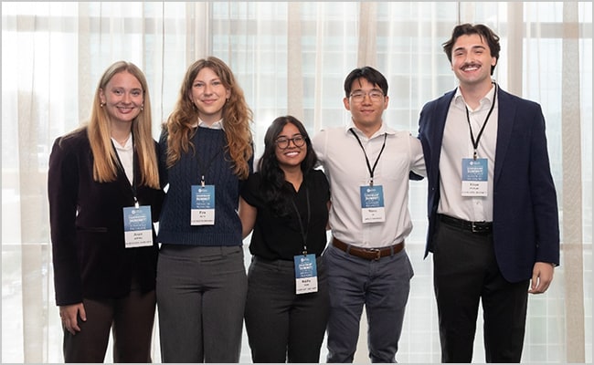
Collaboration alone isn’t enough—we also need talent to fuel progress. Roundtable members highlighted a looming shortage of skilled professionals in advanced packaging. To address this, our Young Workforce Panel brought together industry veterans and emerging engineers for a candid dialogue on what the next generation values: purpose-driven work, flexibility, continuous learning, and hands-on experience.
Building on these insights, participants outlined actionable steps:
- Expand the talent pipeline: Position advanced packaging as “where the action is” with stronger industry branding. Broaden recruitment through sponsored research, campus competitions, and social media.
- Create intentional pathways: Partner with academia to update curricula, offer internships and co-ops, and introduce microelectronics earlier through hands-on labs and dedicated educators.
- Strengthen skills: Align coursework with industry needs by blending hardware and software education. Support interactive learning through apprenticeships, bootcamps, and joint training centers.
“Closing the academia–industry gap is critical to prepare students for AI and system integration… deeper campus partnerships and end-to-end system exposure are essential.”
— Liwei Wang, Senior Director of Heterogeneous Integration, Foundry Technology Development, AMD
Guided by this vision, Applied Materials is strengthening university partnerships, expanding hands-on training, and fostering an inclusive, mentorship-driven culture to support long-term retention.
Looking Ahead
Leaving Phoenix, I felt energized by the shared commitment in the room. It wasn’t just a conversation about technology—it was about trust, transparency, and a common vision for our industry. Together, we can accelerate innovation and build the workforce to sustain it.
For a deeper look, check out our full event report and interviews with attendees. These conversations are shaping the next chapter of advanced packaging—and we look forward to continuing them at the 2026 Leadership Summit in Singapore.

Kevin Moraes
Corporate Vice President, Strategy and Marketing, Semiconductor Products Group

Dr. Kevin Moraes serves as Corporate Vice President of Strategy and Marketing at Applied Materials, leading global initiatives that drive growth across key semiconductor segments. In this role, he aligns market insights with business priorities, shapes competitive positioning, and enables customer success through technology inflections. Previously, he held leadership positions in product management and technology development within the company. He earned a Ph.D. in materials science and engineering from Rensselaer Polytechnic Institute, an MBA from the University of California, Berkeley, and a bachelor’s degree in chemical engineering from Annamalai University.