Products & Technologies
Products & Services
Contact
Products & Services
Products & Technologies
Services
Resources
Contact
Posted
July 01, 2024

Stay updated on our content.
Beyond Backside Power: Scaling Chips to 2nm and Beyond Also Requires Frontside Wiring Innovations
Today’s advanced logic chips have as many as 20 layers of metal that support two types of wires – thin signal wires that switch transistors on and off, and thicker power wires that deliver the current that flows when the transistor is switched on. In the near future, all of the world’s leading chipmakers plan to move the power lines to the backside of the wafer, which promises to reduce wiring complexity, free up space for more transistors, and improve chip performance and power efficiency.
Yet despite the tremendous benefits expected with backside power, we must not forget that we need to address wiring challenges on the front side of the wafer if we hope to scale transistors to 2nm and beyond.
Advances in patterning are making it possible to print ever-smaller transistor features on a chip. But as chipmakers continue to shrink transistors with each generation, they must also shrink the wiring. While it may seem counterintuitive, smaller is not actually better when it comes to wiring.
First, physics dictates that as wires get thinner, electrical resistance increases. Second, as wires get closer together, and the insulating dielectric material between the wires decreases, capacitance and electrical crosstalk increases, resulting in signal delays and distortion. The net effect of these wiring scaling issues is slower and more power-hungry chips.
This is just the opposite of what we need in the AI era of computing. As my colleague Mukund Srinivasan described in last week’s preview of our July 9 SEMICON West Technology Breakfast, the rising demand for AI data center capacity is pushing the need for energy-efficient computing to an entirely new level. If we don’t dramatically improve the efficiency of chips and systems, then the growth of AI computing could be gated by the limits of the power grid.
One of the primary ways our industry has addressed the performance-per-watt challenge is through materials innovation in the smallest wires closest to the transistor layer. More than 20 years ago, the industry introduced “low-k” dielectrics as the insulating materials between wires and replaced aluminum wiring with copper. This combination of low-k dielectrics and copper has been the industry’s workhorse for decades, and we have continually extended this approach by introducing more exotic materials and materials engineering techniques.
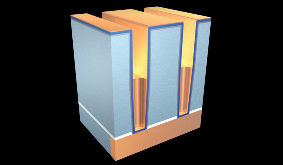
To create wiring, we etch trenches into dielectric material and then line them with a thin stack of metals that typically includes a barrier layer to prevent copper from migrating into the chip, a liner to promote copper adhesion, and finally bulk copper that completes the signal wires.
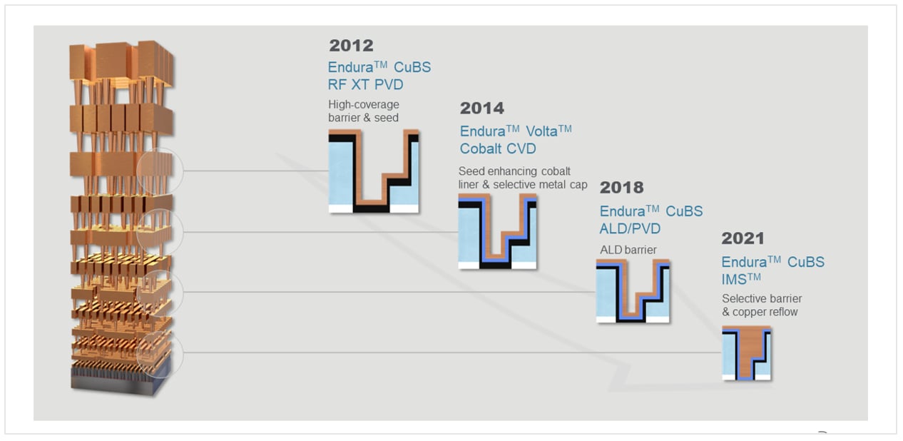
Applied Materials innovations to extend the life of copper interconnects
Continued lithographic scaling shrinks not only transistor features but also the trenches for the wiring. The barriers and liners occupy more of the trench volume, and the remaining space is becoming too narrow to deposit copper without encountering gaps, called voids, which increase resistance and reduce yields. In addition, bringing the wires closer thins the low-k dielectrics and makes the material more susceptible to etch process damage, which increases capacitance while making the chips too weak to withstand 3D stacking. The net result is that just as the industry seeks to move to the 2nm, copper wiring is hitting physical scaling limits.
At next week’s SEMICON West, Applied Materials will unveil innovations designed to extend copper to the 2nm node and below. Register for our technology breakfast to learn more about these and other materials engineering breakthroughs designed to enable better AI.
Mehul Naik, Ph.D.
Master and Vice President of Technology, Semiconductor Products Group

Mehul Naik is a Master and Vice President of Technology with the Advanced Product Technology Development team in the Semiconductor Products Group at Applied Materials. He is responsible for the Logic Program working on inflection mapping and leading cross-functional programs in the FEOL, MEOL and Interconnect area. He has authored over 64 publications and holds over 90 U.S patents. Mehul earned his Ph.D. in chemical engineering from Rensselaer Polytechnic University.