Products & Technologies

Products & Services
Contact
Products & Services
Products & Technologies
Services
Resources
Contact

Stay updated on our content.
Tackling Key HBM and Advanced Packaging Bottlenecks for the AI Era
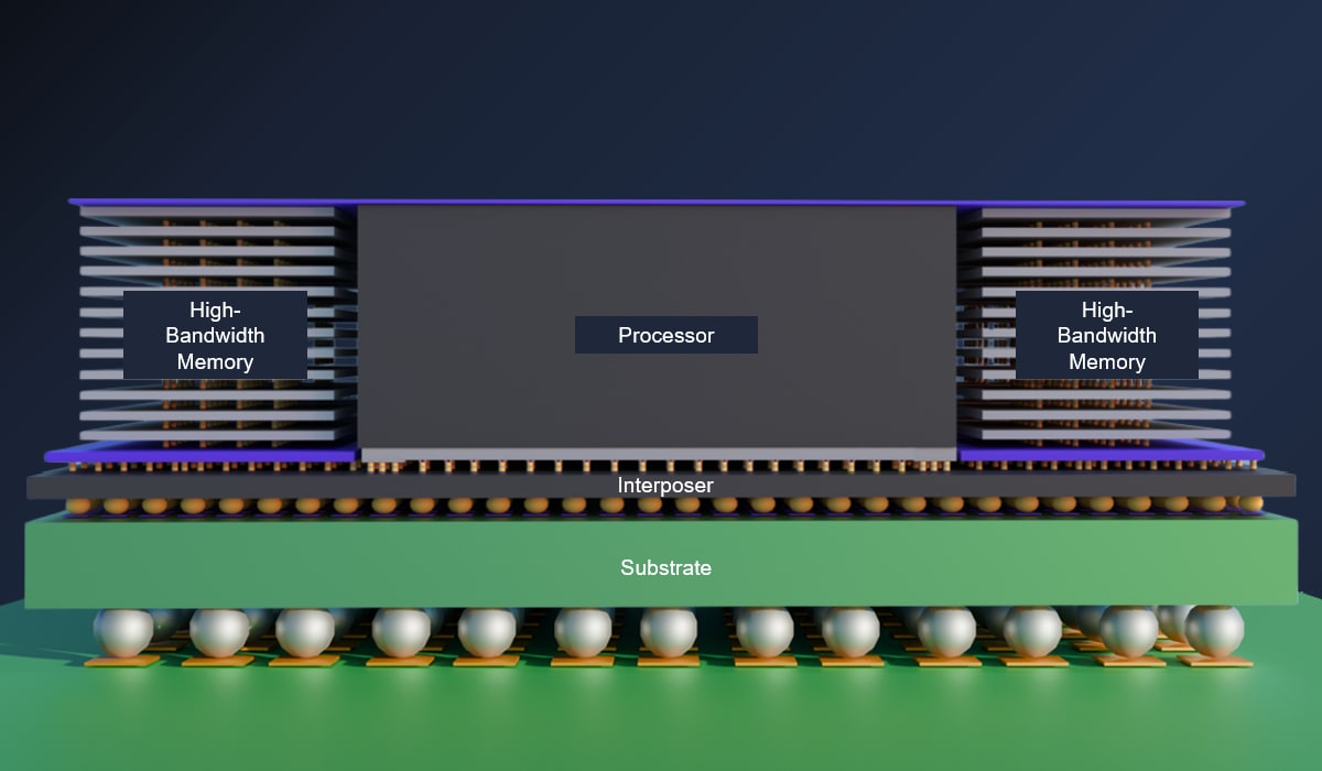
Today's advanced AI processors deliver extraordinary performance but are increasingly limited by how quickly data can move between compute and memory. To overcome this bottleneck, the semiconductor industry is bringing compute and memory closer together, making data transfer faster and more energy efficient.
Consequently, advanced packaging has become a critical enabler of AI scaling. By integrating processors, memory and other chiplets within a tightly interconnected package, it dramatically reduces the distance data must travel. A key example is high-bandwidth memory (HBM), a vertical stack of DRAM dies placed beside a processor on a silicon interposer whose fine wiring connects the two—enabling the massive data throughput required by AI workloads.
As advanced packages incorporate more chiplets, denser interconnects and advanced bonding schemes, they introduce new manufacturing complications. Tackling challenges such as die warpage, fine-pitch wiring formation and bonding precision is essential to scaling systems. Applied recently launched a suite of innovations designed for the most critical advanced packaging inflections.
Improving Wiring Uniformity for Advanced Packages with Nokota™ VMax™ 2 ECD
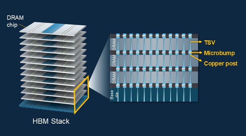
Plating, or electrochemical deposition (ECD), uses electric current to deposit metal into tiny features and onto wafer surfaces, creating the wiring that carries signals and power throughout an advanced package. In HBM, plating is essential for forming both the through-silicon vias (TSVs) within DRAM dies and the microbumps that connect those dies.
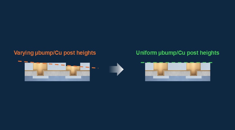
As HBM stacks scale to higher layer counts and wiring dimensions shrink, plating precision becomes especially important for achieving uniform bump coplanarity and high-quality TSV fill. Variations in local feature density can distort current distribution during deposition, leading to non-uniform metal fill.
Applied's Nokota™ VMax™ 2 ECD system is designed for advanced packaging applications, including HBM. Its Adaptive Pattern Tuning (APT) technology dynamically shapes the electric field during deposition to compensate for layout-driven variation, enabling more uniform plating across the wafer.
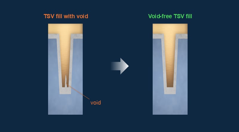
The system achieves highly uniform deposition and void-free metal fill across advanced wiring geometries, including TSVs smaller than 3 microns and deeper than 10:1 aspect ratios. This level of precision is essential in high-layer-count HBM stacks, where interconnect uniformity directly impacts stacking yield, reliability and electrical performance.
Achieving Hybrid Bonding Surface Precision with Opta™ Quad CMP
Today's leading HBM designs use microbumps to connect stacked DRAM dies, while future roadmaps are expected to adopt hybrid bonding for even greater interconnect density. Achieving reliable bonds, however, requires exceptionally flat and uniform wafer surfaces. Even minor surface variations can reduce bond quality, yield and reliability.
Chemical mechanical planarization (CMP) is thus used at multiple points throughout the packaging flow to create the ultra-flat surfaces required for subsequent bonding, including after TSV fill, dielectric deposition and copper pad formation. Compared with front-end applications, packaging CMP involves thicker films, longer polish times and tighter tolerances. Building on Applied's CMP leadership, Opta™ Quad delivers the high throughput and industry-leading planarization needed for these demanding, multi-step flows.
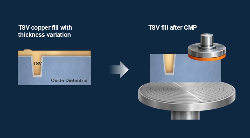
At the system’s core is advanced process control with flexible sequencing. Opta Quad continuously monitors wafer conditions during polishing and makes real-time adjustments to maintain tight thickness uniformity across the wafer. The result is highly stable planarization over extended polish times, delivering the surface precision required for high-yield bonding and HBM manufacturing.
Controlling Warpage in High-Layer HBM with Producer™ Avila™ 2 PECVD
Increasing HBM capacity requires stacking more DRAM dies, which in turn demands thinner dies to stay within package height limits. Today's HBM dies are thinned to roughly 1/25th the thickness of conventional DRAM, making them far more vulnerable to stress, warpage and deformation.
As stack heights grow from 12 layers to 16 layers and beyond, these mechanical challenges compound, increasing the risk of misalignment, bonding defects and yield loss. Controlling stress and warpage is therefore critical to scaling next-generation HBM architectures.
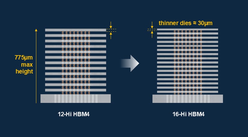
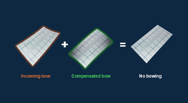
Applied's Producer™ Avila™ 2 PECVD system enables higher-density HBM stacks by improving the mechanical stability of ultra-thin DRAM dies. Leveraging Applied's dielectric CVD leadership, Avila 2 deposits engineered dielectric films that counteract warpage during TSV integration and stabilize the die throughout manufacturing. The resulting stress-balanced film stack enables more reliable bonding and higher yields for next-generation HBM designs.
Scaling the Future of AI Systems
Applied's latest packaging solutions address key manufacturing and yield challenges, helping customers bring next-generation AI systems to market faster and at scale. These systems are complemented by Applied's industry-leading eBeam process control portfolio, including new metrology and defect analysis solutions optimized for the diverse materials, feature sizes and mechanical requirements of advanced packaging.
While today's advanced packages rely on thermocompression bonding with microbumps, the challenges addressed by these systems will become even more critical as the industry transitions to hybrid bonding, where precision and uniformity requirements grow even more stringent. Applied is driving this inflection with Kinex™, the industry's first integrated die-to-wafer hybrid bonding system.
Applied continues to invest in emerging packaging inflections, including panel-based packaging and co-packaged optics, to help enable the industry's future roadmap. Learn more in Applied’s DRAM and Advanced Packaging Masterclass.
Jinho An, Ph.D.
Senior Director, Heterogeneous Integration, Semiconductor Products Group

Jinho An is a Senior Director in the Heterogeneous Integration Business Unit and has been working at Applied Materials as an Account Technologist since 2021. Prior to Applied, he was a process and integration R&D engineer at Samsung Electronics working on wafer level advanced packaging technology and product development including HBM, HD FOWLP, interposers and CIS. Jinho has a B.S. in inorganic materials engineering from Hanyang University and a Ph.D. in materials science and engineering from the University of Texas at Austin.
Kyla Zhao
Product Marketing Manager, Corporate Marketing and Strategy, Semiconductor Products Group

Kyla Zhao is a Product Marketing Manager in the Semiconductor Products Group at Applied Materials. She spearheads strategic messaging and content leadership that highlight how advances in materials engineering, process innovation and semiconductor equipment enable the next generation of technology. Kyla holds both a Master's degree and a Bachelor's degree from Stanford University.