Products & Technologies

Products & Services
Contact
Products & Services
Products & Technologies
Services
Resources
Contact

Stay updated on our content.
Bringing Next-Generation CD-SEM Metrology to the Fab
August 31, 2026
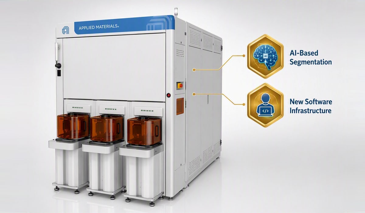
Applied VeritySEM™ 20 Critical Dimension Metrology
Why the Industry Needs a New Approach
The semiconductor industry is at an inflection point. Logic, DRAM, and NAND devices continue to push the limits of scaling, and manufacturers are seeking new ways to improve device performance and yield while lowering cost of ownership. As High-NA EUV lithography moves from concept to high-volume manufacturing, fabs face new challenges that can affect yield, cycle time, and cost.
As the High-NA EUV era progresses, traditional critical dimension scanning electron microscopes (CD-SEMs) must evolve. Chipmakers need a CD-SEM capable of accurately measuring thinner resists, supporting tighter process windows, and enabling faster recipe creation—all without compromising fleet stability. To meet these evolving requirements, Applied Materials® developed the VeritySEM 20, a next-generation CD-SEM metrology system designed to extend patterning control into the High-NA EUV era.
What’s Changing Inside the Fab
Launched in 2023, the VeritySEM 10 marked a significant step forward in EUV metrology and has been widely adopted by semiconductor manufacturers worldwide. Building on this foundation, VeritySEM 20 is designed to address the growing complexity of the High-NA EUV era. Thinner and more diverse photoresists, combined with evolving device architectures, introduce new imaging challenges: electron-material interactions can cause measurement-induced shrinkage and inaccuracies during resist development, while resist outgassing can affect long-term tool stability and fleet matching. At the same time, continued feature shrink tightens process windows, requiring greater precision and matching to sustain device performance and yield. Cost of ownership also matters more than ever, with time-to-recipe, ease of use, and tool availability central to fab economics.
How VeritySEM 20 Innovation Makes It Possible
VeritySEM 20 is engineered to meet these evolving requirements through advanced metrology innovations and AI-driven process efficiencies. For High-NA EUV advanced metrology applications, a wider landing energy range and integrated chamber-cleaning capabilities enable contamination-free metrology of ultra-thin resists. New shape metrics support stochastics characterization and monitoring, while multi-directional scanning for charge control helps stabilize imaging and deliver a 20–50% throughput improvement. VeritySEM 20 also delivers precision and matching improvements of up to 25%, enabling tighter process control at fleet scale. To accelerate development cycles, AI-driven recipe optimization improves measurement robustness, reduces user-to-user variation, and enhances ease of use. In parallel, a new software infrastructure with CAD-based waferless recipe creation introduces an intuitive workflow that shortens time-to-recipe and accelerates process development without consuming valuable wafer or tool time.
A key part of that AI capability is a deep learning segmentation engine built into the system’s software — the part that picks out the edges of each feature in an image so it can be measured. Because it was trained in advance on a large, varied set of images, it arrives ready to work: no training in the fab and no manual tuning. It runs on the tool itself and can measure a new layer the first time it sees one. It also holds up on the difficult images — grainy ones, or wafers with large process variation — that conventional algorithms miss. The result is more reliable measurements, consistent results from one engineer to the next, and a simpler tool to run — all of which lowers total cost of ownership for customers.
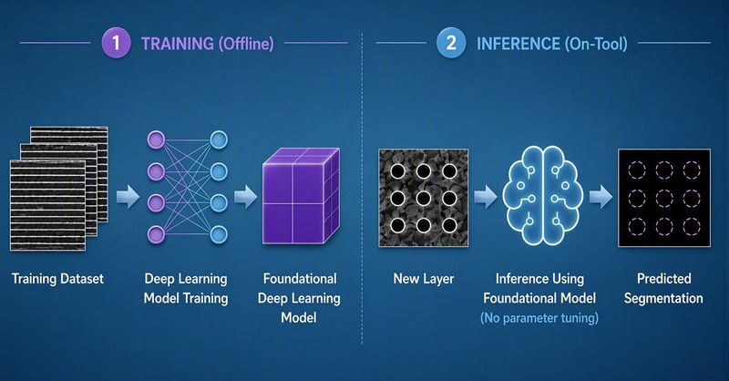
Applied VeritySEM 20 deep learning segmentation: the foundational model is trained offline, then runs on-tool to segment a new layer with no parameter tuning.
Why This Matters for Customers
For customers, VeritySEM 20 ultimately means measurements they can trust on the hardest layers, consistent results from one engineer to the next, and a shorter path from a new layer to a qualified recipe — gains that compound as they scale advanced logic and memory devices. Just as important, that performance holds at fleet scale, where precision, matching, and tool availability drive both yield and cost of ownership. As device architectures continue to evolve, VeritySEM 20 extends Applied Materials’ leadership in process control.