Products & Technologies

Products & Services
Contact
Products & Services
Products & Technologies
Services
Resources
Contact

Stay updated on our content.
Breaking Scaling Barriers in 3D Chips with Robust ALD SiN Films
July 13, 2026
By Ramkumar Vinnakota

To meet the performance and energy demands of AI, the industry is rapidly shifting to advanced 3D architectures, including gate-all-around (GAA) transistors in advanced logic and deep channels in next-generation memory. As these designs evolve, features are becoming taller, narrower, and more complex. This makes controlling materials at the atomic scale a key bottleneck to continued scaling.
Silicon nitride (SiN) is one of the most widely used insulating materials across logic and memory. Robust SiN liners are needed to preserve feature fidelity during aggressive downstream processing. However, conventional plasma-enhanced atomic layer deposition (PE-ALD) struggles to deposit high-quality SiN deep in 3D structures without damaging sensitive device layers.
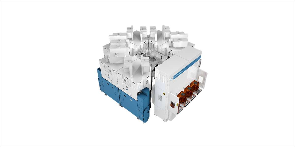
Applied Materials addresses this challenge with Centris™ Spectral™ SiN ALD, purpose-built for the most demanding 3D architectures. Using a breakthrough microwave plasma technology, it creates SiN films that improve performance, power efficiency and yield across logic and memory scaling.
Limitations of Conventional Plasma Deposition
As the industry moved from planar to FinFET and GAA architectures, thermal budgets tightened, driving adoption of low-temperature PE-ALD. But as 3D structures reach aspect ratios of 6:1 and beyond, conventional PE-ALD becomes increasingly limited in its ability to uniformly coat these features. It delivers too few reactive species to fully reach all surfaces, while its high-energy ions risk damaging sensitive materials. Attempts to reduce ion energy often come at the expense of plasma density, creating a fundamental tradeoff between coverage and damage.
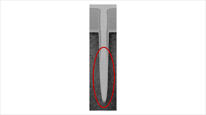
Weaker films are more susceptible to downstream erosion in high-aspect-ratio features
The result is non-uniform films with insufficient robustness to withstand downstream chipmaking processes, ultimately degrading device performance and yield. As 3D scaling accelerates, the industry needs a new approach that can simultaneously deliver:
- high plasma density
- low ion energy
- uniform deposition deep within complex structures
A Breakthrough in Plasma Technology
Spectral SiN ALD introduces Nimbus™, a high-density direct microwave plasma technology that overcomes these long-standing limitations. Nimbus generates a high volume of gentle reactive species, breaking the longstanding tradeoff between plasma density and ion-induced damage.
Spatial ALD maximizes benefits of Nimbus™ direct microwave plasma technology
Furthermore, Spectral utilizes a unique spatial architecture that separates ALD processing into distinct zones to fully realize the benefits of the direct microwave technology. In one zone, precursor gases create a uniform adsorbed layer; in another, optimized plasma conditions activate and densify the deposited chemistry into a high-quality film. By decoupling these steps, each can be precisely tuned for maximum performance.
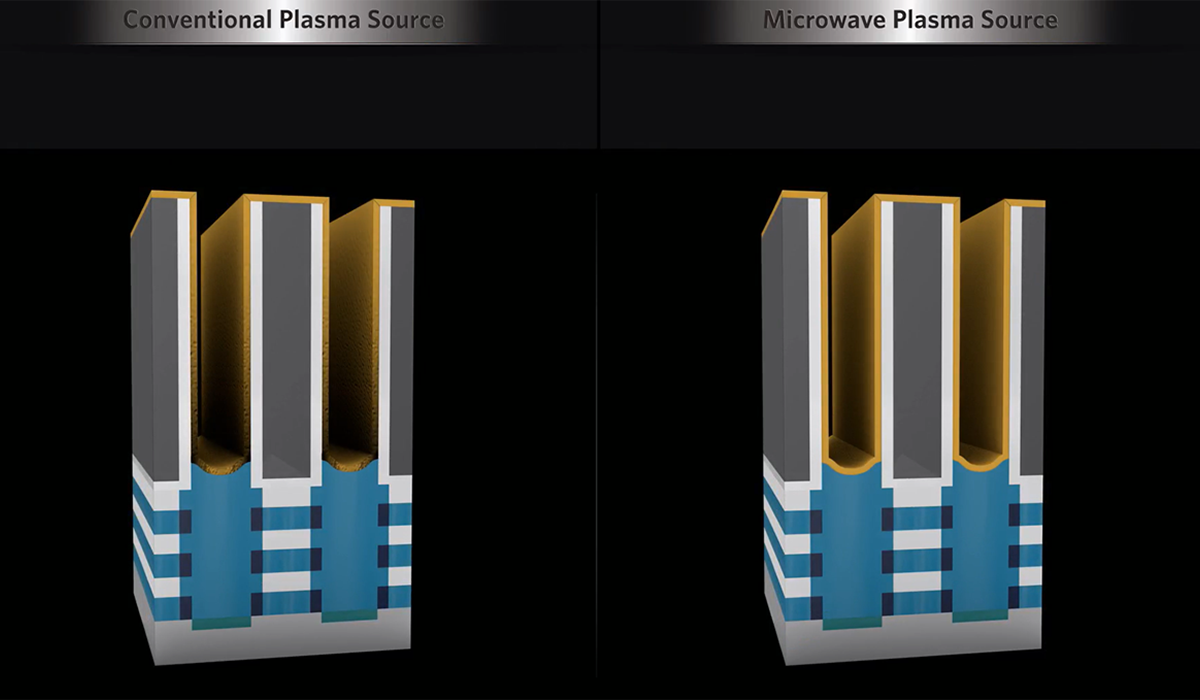
Compared to conventional PE-ALD, the films created with Spectral SiN ALD deliver up to 5x higher resistance to downstream etch in high-aspect-ratio structures. This capability is a critical enabler for next-generation 3D architectures in both logic and memory.
In advanced GAA logic devices, for example, Spectral SiN ALD forms high-quality liners at key interfaces, such as the contact-to-source/drain junction. These liners preserve contact geometry during downstream processing while reducing resistance and parasitic capacitance. This ultimately improves switching speed and overall transistor performance, which are essential for high-performance AI processors.
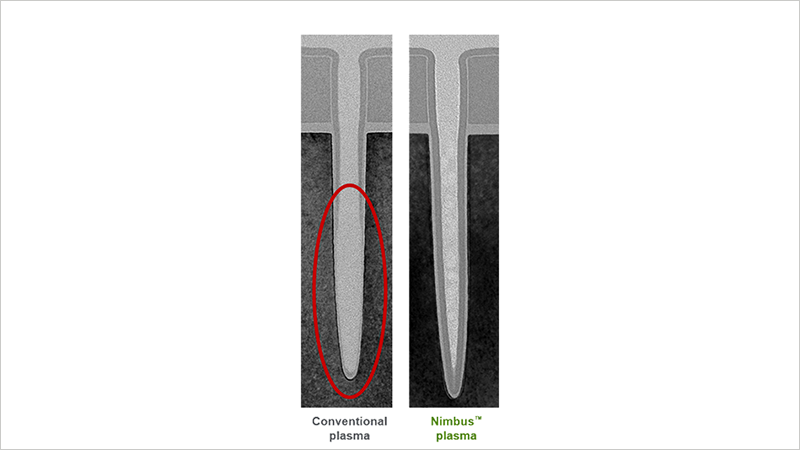
Films created with Spectral SiN ALD are more resistant to erosion from downstream processing.
Advancing Applied’s Leadership in Materials Engineering
Spectral SiN ALD is already in production at leading chipmakers. Built on the Centris™ Spectral™ quad‑reactor platform, it extends Applied’s ALD leadership and complements adjacent technologies such as Spectral Mo ALD (for metal fill in logic contacts at 2nm and beyond). As AI drives increasingly complex chip designs, Spectral SiN ALD reinforces Applied’s role at the center of next‑generation semiconductor innovation and AI scaling.
Ramkumar Vinnakota
Global Product Manager, Dielectric Atomic Layer Deposition (ALD)

Ramkumar Vinnakota is the head of product management for the Dielectric ALD business unit at Applied Materials. Since joining Applied in 2016, Ramkumar has held product management roles spanning ALD, CVD and PVD technologies used in advanced semiconductor manufacturing. Prior to Applied, Ramkumar worked at Lam Research as an etch process manager.