Products & Technologies

Products & Services
Contact
Products & Services
Products & Technologies
Services
Resources
Contact

Stay updated on our content.
Advancing DRAM Performance With Logic-Class Technologies
July 27, 2026
By Sony Varghese, Ph.D.

DRAM—including HBM—has become the performance-critical memory technology for modern AI systems. As demand for compute continues to surge, the industry faces a new challenge: how to advance DRAM performance as scaling becomes increasingly difficult.
A DRAM chip consists of two primary elements: the memory cell array, which stores data, and the periphery circuitry, which reads, writes, processes and moves that data. Historically, DRAM improvements were driven largely by shrinking memory cells so more bits could be packed into each DRAM die. But as the pace of cell scaling slows, DRAM innovation is also shifting to the peripheral circuitry.
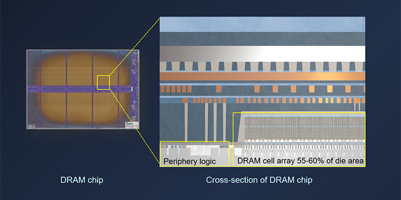
That shift is driving DRAM manufacturers to adopt technologies long associated with leading-edge logic. Epitaxy-based materials engineering, advanced transistor architectures and sophisticated interconnect schemes are emerging as critical new levers for extending DRAM performance in the AI era.
Bringing Logic-Class Epitaxy to DRAM
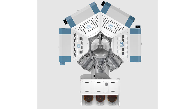
Epitaxy has long been one of the semiconductor industry's most effective performance boosters. As transistor dimensions continue to shrink, drive current naturally declines. By precisely engineering doped regions in the transistor, chipmakers can offset this effect by enhancing transistor performance without increasing device footprint. In DRAM periphery transistors, a key application is embedded silicon germanium (SiGe) in the channel, enabled by Applied Materials' Centura™ Prime™ Epi system.
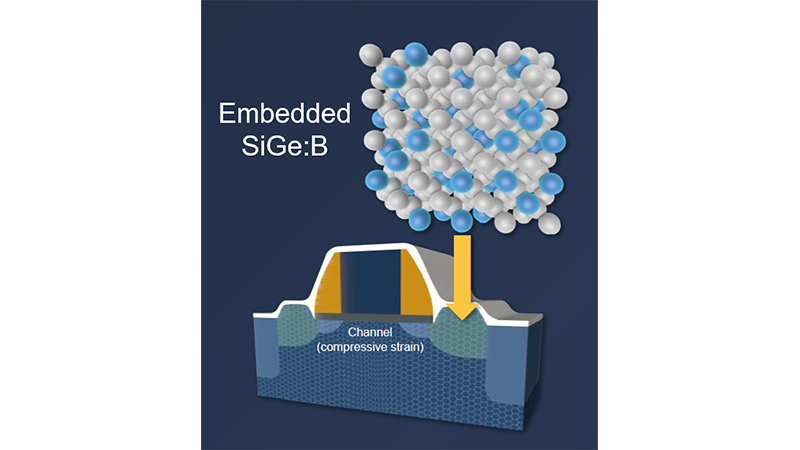
Building on this capability, Applied recently introduced a new epitaxy step on the enhanced Centura Prime Epi: boron-doped embedded SiGe in the source/drain. Since SiGe has a larger lattice constant than silicon, it wants to expand. However, the surrounding silicon constrains that expansion, inducing compressive strain in the adjacent transistor channel. This strain boosts carrier mobility, allowing current to flow more easily. Boron doping further improves electrical conductivity, delivering an added performance boost.
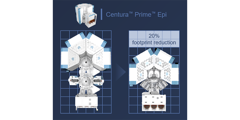
Together, these advances help DRAM deliver faster data access, higher bandwidth, better signal integrity, and improved energy efficiency. To help customers maximize output, the enhanced Centura Prime Epi platform also features a 20% smaller footprint optimized for DRAM fabs, where floor space is becoming increasingly valuable as AI-driven memory demand accelerates.
CMOS-Bonded Array Architecture Increases Wiring Complexity
As DRAM manufacturers continue scaling, they are integrating more memory cells and peripheral circuitry onto every chip. The shift to CMOS-bonded array (CBA) architectures is accelerating this trend. By separating the memory array and peripheral circuitry onto different wafers and then bonding them together, CBA enables each to be independently optimized with separate thermal budgets and process constraints. However, the resulting architecture requires many more data pathways between the wafers, driving greater routing complexity.
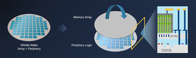
To support this increasingly routing-intensive architecture, DRAM manufacturers are adding more copper interconnect layers and adopting advanced metallization and dielectric schemes, mirroring a scaling path previously taken by leading-edge logic.
Combined with AI's insatiable demand for bandwidth, these additional wiring layers are becoming critical to performance—and elevating the importance of advanced wiring technologies, an area where Applied has led the industry for decades.
FinFETs Come to Memory
In the periphery circuitry, DRAM manufacturers are transitioning from traditional planar transistors to FinFET architectures. Already proven in leading-edge logic for over a decade, FinFETs offer several advantages for continued DRAM scaling. Their compact structure supports higher transistor density, while superior electrostatic control improves performance and reduces leakage.
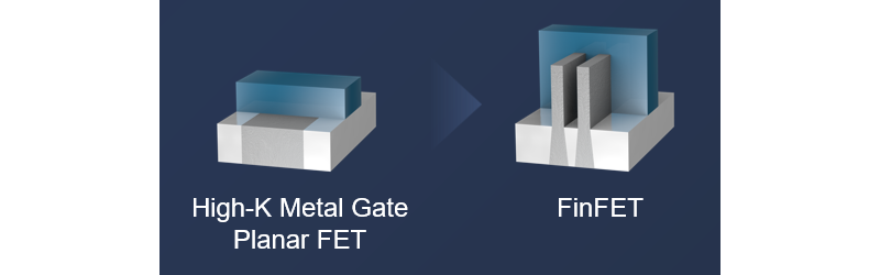
Moreover, critical device dimensions in FinFETs are defined through highly precise lithography and etch processes, helping reduce transistor-to-transistor variability. This is particularly important in DRAM periphery circuits, where sense amplifiers must detect extremely small voltage differences representing stored data. By delivering more uniform transistor characteristics, FinFETs help preserve sensing margins and reliability.
These benefits become even more compelling with the adoption of CBA architectures. The high temperatures required to fabricate DRAM capacitors can degrade transistor performance. With periphery circuitry built on a separate wafer, manufacturers can fully capture the performance, power, and scaling advantages of advanced FinFET transistors.
A New Era for DRAM Scaling
As DRAM advances beyond conventional cell scaling, manufacturers are increasingly adopting the materials-engineering innovations that powered leading-edge logic. The convergence of logic and memory is expanding the range of advanced process technologies required to manufacture next-generation DRAM—and positions Applied Materials at the center of both markets.
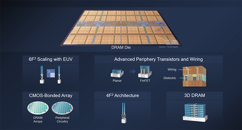
The adoption of logic-class technologies and the CBA architecture are among the five major DRAM inflections that Applied is enabling with our leadership in materials engineering. To learn more, explore our DRAM and Advanced Packaging Master Class.
Sony Varghese
Managing Director of Technology Strategy, Semiconductor Products Group

Dr. Sony Varghese is Managing Director of Technology Strategy for next-gen products in the Semiconductor Products Group at Applied Materials. In this role, he is involved in identifying future key inflections and challenges to scaling advanced semiconductors in Applied’ s implant and patterning business units. Prior to Applied Materials, he worked on developing various memory technologies within the R&D organization at Micron Technology. Dr. Varghese has over 60 U.S. patents issued or pending in the area of semiconductor processing and integration. He has a Ph.D. in materials and mechanical engineering from Oklahoma State University.